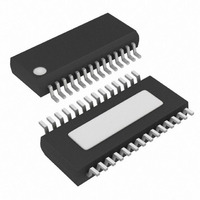
MAX8513EEI+ Maxim Integrated Products, MAX8513EEI+ Datasheet - Page 27

MAX8513EEI+
Manufacturer Part Number
MAX8513EEI+
Description
IC SUPPLY TRPL W/MON 28QSOP
Manufacturer
Maxim Integrated Products
Type
Step-Down (Buck)r
Datasheet
1.MAX8513EEIT.pdf
(35 pages)
Specifications of MAX8513EEI+
Internal Switch(s)
No
Synchronous Rectifier
No
Number Of Outputs
3
Voltage - Output
1.25 ~ 5.5 V
Current - Output
40mA
Frequency - Switching
300kHz ~ 1.4MHz
Voltage - Input
4.5 ~ 28 V
Operating Temperature
-40°C ~ 85°C
Mounting Type
Surface Mount
Package / Case
28-QSOP
Power - Output
860mW
Lead Free Status / RoHS Status
Lead free / RoHS Compliant
Use 47pF.
The MAX8513/MAX8514 OUT2 positive linear regula-
tor’s output voltage is set by connecting a resistive-
divider from OUT2 to FB2 to GND. The resistors in the
divider are selected to set the minimum output current
(I
5 or Figure 6), the feedback resistors are set to R5 =
340Ω and R6 = 160Ω, where R5 is the resistor from
OUT2 to FB2 and R6 is the resistor from FB2 to GND.
These values set the minimum output current to
≈4.5mA, which works well with many MOSFETS.
In general,
Select R5 and R6 so:
A transconductance amplifier drives the gate of the
NMOS transistor (Q3 in the Typical Applications
Circuits), with current proportional to the error signal
multiplied by the amplifier’s transconductance. The
error signal is the difference between V
internal 0.8V reference. V
the transconductance amplifier, must be at least 1V
greater than the maximum required gate voltage
(V
DRV2 signal to produce the desired output voltage
(V
Applications Circuits) helps bypass the output, while
Wide-Input, High-Frequency, Triple-Output Supplies
OUT2_MIN
DRV2
OUT2
C
). The output pass transistor (Q3) buffers the
12
). The output capacitor (C6 in the Typical
Linear-Regulator Controllers
=
=
). For the Typical Applications Circuit (Figure
I
(
2
OUT
2
π
π
×
×
R
2
12
C
5
_
0 8
______________________________________________________________________________________
R
MIN
nF
5
.
6
=
×
C
V
with Voltage Monitor and Power-On Reset
×
R
5
R
=
20
3
12
=
6
OUT2 Voltage Selection
×
I
k
nF
OUT
×
SUP2
f
I
Ω
P
OUT
3
×
V
)
2
150
0 8
-
OUT
333
1
2
, the supply voltage for
_
.
_
MIN
V
MAX
kHz
2
-
OUT2 Stability
1
-
1
=
53 3
FB2
.
pF
and the
the feedback resistors (R5 and R6) set the output-volt-
age reference point as well as the minimum load.
The loop gain for the positive LDO output using an
NMOS transistor is:
where C
G
(0.21S typ), and a dominant pole at a low frequency is
created from this transconductance and the compen-
sation capacitor (C
+ Q3’s gate capacitance (C
due to C
This transconductance varies from a minimum g
occurring at minimum load to a maximum g
occurring at maximum load. To calculate the g
load current, the typical forward transconductance can
be extracted from the MOSFET’s data sheet (gfs), as
well as the current at which it is measured (IDfs). The
g
Poles occur at:
If only a minimum gfs is given, initially assume the max-
imum is twice the minimum.
When using a bipolar transistor, the g
g
where V
C(MIN)
C(MIN)
C2
V
is the transconductance of the internal amplifier
0 8
OUT
. V
T
OUT2
and g
occur at the following:
OUT2
is the thermal voltage, 26mV.
2
×
g
g
f
and f
PMAX
s CA Cq
is C6 in the Typical Applications Circuits.
C(MAX)
C MAX
C MIN
(
and the transconductance of Q3 (g
(
(
g
g
C MIN
C MAX
(
(
PMIN
A
+
)
)
=
in the Typical Applications Circuits
can be calculated as:
=
)
=
)
2
G
)
gfs
=
π
=
gfs
g
=
C
1
×
+
C MAX
2
I
(
2
OUT MIN
(
C
I
1
sC
OUT MAX
q
π
I
OUT MIN
OUT
g
+
)). A second pole occurs
I
OUT MAX
×
V
g
C MIN
OUT
sCA RA
V
2
T
C
C
IDfs
(
)
2
T
IDfs
2
2
OUT
2
(
2
(
×
)
+
(
2
1
)
)
)
sRA Cq
C(MAX)
×
C
C(MAX)
C(MIN)
at any
)
and
C
27
).


