MAX8561ETA+T Maxim Integrated Products, MAX8561ETA+T Datasheet - Page 6
MAX8561ETA+T
Manufacturer Part Number
MAX8561ETA+T
Description
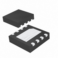
IC DC-DC CONV ADJ 500MA 8-TDFN
Manufacturer
Maxim Integrated Products
Type
Step-Down (Buck)r
Datasheet
1.MAX8560EZKT.pdf
(12 pages)
Specifications of MAX8561ETA+T
Internal Switch(s)
Yes
Synchronous Rectifier
Yes
Number Of Outputs
1
Voltage - Output
0.6 ~ 2.5 V
Current - Output
500mA
Frequency - Switching
4MHz
Voltage - Input
2.7 ~ 5.5 V
Operating Temperature
-40°C ~ 85°C
Mounting Type
Surface Mount
Package / Case
8-TDFN Exposed Pad
Power - Output
1.95W
Lead Free Status / RoHS Status
Lead free / RoHS Compliant


4MHz, 500mA Synchronous Step-Down
DC-DC Converters in Thin SOT and TDFN
The MAX8560/MAX8561/MAX8562 step-down converters
deliver a guaranteed 500mA at output levels from 0.6V to
2.5V. They use a proprietary hysteretic-PWM control
scheme that switches up to 4MHz, allowing a trade-off
between efficiency and tiny external components. At light
loads below 100mA, the MAX8560/MAX8561/MAX8562
automatically switch to pulse-skipping mode to keep qui-
escent supply current as low as 40µA (typ).
A proprietary hysteretic-PWM control scheme ensures
high efficiency, fast switching, fast transient response,
low output ripple, and physically tiny external compo-
nents. This control scheme is simple: when the output
voltage falls below the regulation threshold, the error
comparator begins a switching cycle by turning on the
high-side switch. This switch remains on until the mini-
mum on-time expires and the output voltage is in regu-
lation or the current-limit threshold is exceeded. Once
off, the high-side switch remains off until the minimum
off-time expires and the output voltage falls again,
6
MAX8560
_______________________________________________________________________________________
—
—
—
—
1
2
3
4
5
PIN
MAX8561
MAX8562
EP
1
7
8
6
2
3
5
4
Detailed Description
NAME
SHDN
PGND
GND
ODO
ODI
FB
LX
EP
IN
Control Scheme
Supply Voltage Input. 2.7V to 5.5V. Bypass with a 2.2µF ceramic capacitor as close as
possible to the IN and GND pins.
Ground
Active-Low Shutdown Input. Connect to IN or logic high for normal operation. Connect to
GND or logic low for shutdown mode.
Voltage Feedback Input. FB regulates to 0.6V nominal. Connect FB to the center of an
external resistive divider (see the Setting the Output Voltage section).
Power Ground. Must connect to GND.
Inductor connection to the drains of the internal P-channel and N-channel MOSFETs.
Auxiliary Open-Drain Output
Digital Input for Open-Drain MOSFET. Connect to IN or logic high to internally pull ODO
low (and force the MAX8562 into 100% duty cycle). Connect to GND or logic low to force
ODO to high impedance (MAX8561) or 10kΩ pullup from ODO to IN (MAX8562).
Exposed Pad. Connect to GND.
below the regulation threshold. During this period, the
low-side synchronous rectifier turns on and remains on
until either the high-side switch turns on again or the
inductor current approaches zero. The internal syn-
chronous rectifier eliminates the need for an external
Schottky diode.
As seen in the Typical Operating Circuit, the
MAX8560/MAX8561/MAX8562 use a unique feedback
network. By taking feedback from the LX node through
R1, the usual phase lag due to the output capacitor is
removed, making the loop exceedingly stable and
allowing the use of a very small ceramic output capaci-
tor. This configuration causes the output voltage to shift
by the inductor series resistance multiplied by the load
current. This voltage-positioning load regulation greatly
reduces overshoot during load transients, which effec-
tively halves the peak-to-peak output-voltage excur-
sions compared to traditional step-down converters.
See the Load Transient Response graph in the Typical
Operating Characteristics section.
Voltage-Positioning Load Regulation
FUNCTION
Pin Description
Related parts for MAX8561ETA+T
Image
Part Number
Description
Manufacturer
Datasheet
Request
R

Part Number:
Description:
MAX7528KCWPMaxim Integrated Products [CMOS Dual 8-Bit Buffered Multiplying DACs]
Manufacturer:
Maxim Integrated Products
Datasheet:
Part Number:
Description:
Single +5V, fully integrated, 1.25Gbps laser diode driver.
Manufacturer:
Maxim Integrated Products
Datasheet:
Part Number:
Description:
Single +5V, fully integrated, 155Mbps laser diode driver.
Manufacturer:
Maxim Integrated Products
Datasheet:
Part Number:
Description:
VRD11/VRD10, K8 Rev F 2/3/4-Phase PWM Controllers with Integrated Dual MOSFET Drivers
Manufacturer:
Maxim Integrated Products
Datasheet:
Part Number:
Description:
Highly Integrated Level 2 SMBus Battery Chargers
Manufacturer:
Maxim Integrated Products
Datasheet:
Part Number:
Description:
Current Monitor and Accumulator with Integrated Sense Resistor; ; Temperature Range: -40°C to +85°C
Manufacturer:
Maxim Integrated Products
Part Number:
Description:
TSSOP 14/A�/RS-485 Transceivers with Integrated 100O/120O Termination Resis
Manufacturer:
Maxim Integrated Products
Part Number:
Description:
TSSOP 14/A�/RS-485 Transceivers with Integrated 100O/120O Termination Resis
Manufacturer:
Maxim Integrated Products
Part Number:
Description:
QFN 16/A�/AC-DC and DC-DC Peak-Current-Mode Converters with Integrated Step
Manufacturer:
Maxim Integrated Products
Part Number:
Description:
TDFN/A/65V, 1A, 600KHZ, SYNCHRONOUS STEP-DOWN REGULATOR WITH INTEGRATED SWI
Manufacturer:
Maxim Integrated Products
Part Number:
Description:
Integrated Temperature Controller f
Manufacturer:
Maxim Integrated Products
Part Number:
Description:
SOT23-6/I�/45MHz to 650MHz, Integrated IF VCOs with Differential Output
Manufacturer:
Maxim Integrated Products
Part Number:
Description:
SOT23-6/I�/45MHz to 650MHz, Integrated IF VCOs with Differential Output
Manufacturer:
Maxim Integrated Products
Part Number:
Description:
EVALUATION KIT/2.4GHZ TO 2.5GHZ 802.11G/B RF TRANSCEIVER WITH INTEGRATED PA
Manufacturer:
Maxim Integrated Products
Part Number:
Description:
QFN/E/DUAL PCIE/SATA HIGH SPEED SWITCH WITH INTEGRATED BIAS RESISTOR
Manufacturer:
Maxim Integrated Products
Datasheet: