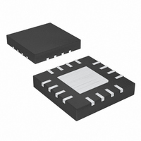
MAX5092AATE+T Maxim Integrated Products, MAX5092AATE+T Datasheet

MAX5092AATE+T
Specifications of MAX5092AATE+T
Related parts for MAX5092AATE+T
MAX5092AATE+T Summary of contents
Page 1
... Automotive—ECU Industrial Typical Operating Circuit and Selector Guide appear at end of data sheet. ________________________________________________________________ Maxim Integrated Products For pricing, delivery, and ordering information, please contact Maxim Direct at 1-888-629-4642, or visit Maxim’s website at www.maxim-ic.com. o Wide Operating Input Voltage Range: 3.5V to 72V with a 4V Startup Voltage o LDO Output Regulates to 5V Seamlessly from an Input Voltage of 3 ...
Page 2
Input LDOs with Boost Preregulator ABSOLUTE MAXIMUM RATINGS IN, EN, LX, BSOUT to SGND..................................-0.3V to +80V PGND_BST, PGND_LDO to SGND .......................-0.3V to +0.3V RESET, OUT, OUT_SENSE to SGND .....................-0.3V to +12V BSOUT to LX (MAX5092_)......................................-0.3V to +12V ...
Page 3
Input LDOs with Boost Preregulator ELECTRICAL CHARACTERISTICS (continued 14V 1mA 47µ OUT IN noted. See Figures 4–7 as applicable. Typical specifications are at T PARAMETER SYMBOL ...
Page 4
Input LDOs with Boost Preregulator ELECTRICAL CHARACTERISTICS (continued 14V 1mA 47µ OUT IN noted. See Figures 4–7 as applicable. Typical specifications are at T PARAMETER SYMBOL ...
Page 5
Input LDOs with Boost Preregulator ( 14V 47µ BSOUT applicable.) QUIESCENT SUPPLY CURRENT vs. INPUT VOLTAGE (MAX5092B 100μA OUT ...
Page 6
Input LDOs with Boost Preregulator ( 14V 47µ BSOUT applicable.) LINE-TRANSIENT RESPONSE (V STEP FROM 4V TO 7V) IN MAX5092/93 toc09 I OUT V OUT 50mV/div V IN ...
Page 7
Input LDOs with Boost Preregulator ( 14V 47µ BSOUT applicable.) POWER-SUPPLY REJECTION RATIO vs. FREQUENCY 8V -70 100 1k 10k 100k FREQUENCY (Hz) ...
Page 8
Input LDOs with Boost Preregulator ( 14V 47µ BSOUT applicable.) V vs. TEMPERATURE OUT 3.36 3.34 3.32 3.30 3.28 3. 10mA 100kΩ, OUT R4 ...
Page 9
Input LDOs with Boost Preregulator PIN NAME Input Supply Voltage. Bypass IN to the power ground plane with a 47µF (low-ESR) aluminum electrolytic 1 IN capacitor in parallel with a 1µF ceramic capacitor placed as close to ...
Page 10
Input LDOs with Boost Preregulator MAX5092_ ONE-SHOT OUT 2.25μs ONE-SHOT OUT IN BSOUT V DIS_TH BST_DIS OUT HOLD CONTROL LOGIC, THERMAL SHUTDOWN, AND OVERCURRENT EN PROTECTION CT COMPARATOR 0. REF Figure 1. MAX5092_ Functional Diagram ...
Page 11
Input LDOs with Boost Preregulator MAX5093_ ONE-SHOT OUT 2.25μs ONE-SHOT OUT IN BSOUT V DIS_TH BST_DIS OUT HOLD CONTROL LOGIC, THERMAL SHUTDOWN, AND OVERCURRENT EN PROTECTION CT COMPARATOR 0. REF Figure 2. MAX5093_ Functional Diagram ...
Page 12
Input LDOs with Boost Preregulator Detailed Description The MAX5092A/MAX5092B/MAX5093A/MAX5093B include a step-up, switch-mode DC-DC converter and a linear regulator to provide step-up/-down voltage con- version over a wide range of input voltages. This combi- nation of an ...
Page 13
Input LDOs with Boost Preregulator Internal Regulator (VL) An internal regulator (VL) is used to supply all internal low-voltage blocks. Bypass VL to SGND with a 1µF ceramic capacitor placed as close to the IC as possi- ...
Page 14
Input LDOs with Boost Preregulator INPUT 4V TO 72V C1* 47μF VOUT RESET ON OFF *** P *THESE CAPACITORS MUST BE RATED AT THE HIGHEST V **OUTPUT CURRENT IS LIMITED BY THE TOTAL POWER-DISSIPATION CAPABILITY OF THE ...
Page 15
Input LDOs with Boost Preregulator INPUT 4V TO 72V C1* 47μF VOUT RESET ON OFF *** P *THESE CAPACITORS MUST BE RATED AT THE HIGHEST V **OUTPUT CURRENT IS LIMITED BY THE TOTAL POWER-DISSIPATION CAPABILITY OF THE ...
Page 16
Input LDOs with Boost Preregulator INPUT 4V TO 72V C1* 47μF VOUT RESET ON OFF *** P *THESE CAPACITORS MUST BE RATED AT THE HIGHEST V **OUTPUT CURRENT IS LIMITED BY THE TOTAL OUTPUT POWER AND THE ...
Page 17
Input LDOs with Boost Preregulator 4.7μH INPUT 4V TO 72V C1* 47μF VOUT RESET ON OFF *** P *THESE CAPACITORS MUST BE RATED AT THE HIGHEST V **OUTPUT CURRENT IS LIMITED BY THE TOTAL OUTPUT POWER AND ...
Page 18
Input LDOs with Boost Preregulator Design Guidelines Input Capacitor (C Boost Capacitor (C BSOUT The input current waveform of the boost converter is continuous, and usually does not demand high capaci- tance at its input. However, the ...
Page 19
... The glitch immunity delay is directly proportional to the CT capacitor and is approximately 70µs for a 0.1µF capacitor at CT. ⎞ − 1 ⎟ ⎠ Dual Mode is a trademark of Maxim Integrated Products, Inc. CT Capacitor Selection ) is out of regulation. When OUT ) from CT to SGND (Figures 4–7). For calculate DELAY − ...
Page 20
Input LDOs with Boost Preregulator MAXIMUM POWER DISSIPATION vs. AMBIENT TEMPERATURE 3.0 2.5 2.0 1.5 1.0 0.5 0 -40 -25 - AMBIENT TEMPERATURE (°C) Figure 8. MAX5092/MAX5093 Package Power Dissipation Maximum Output Current ...
Page 21
Input LDOs with Boost Preregulator INPUT 4V TO 72V VOUT RESET OUTPUT ENABLE * P *SEE PCB LAYOUT GUIDELINES SECTION. PRESET LDO PART OUTPUT (V) MAX5092AATE+ 3.3 MAX5092BATE+ 5 MAX5093AATE+ 3.3 MAX5093BATE+ 5 ______________________________________________________________________________________ ...
Page 22
Input LDOs with Boost Preregulator (The package drawing(s) in this data sheet may not reflect the most current specifications. For the latest package outline information go to www.maxim-ic.com/packages.) 22 ______________________________________________________________________________________ Package Information ...
Page 23
Input LDOs with Boost Preregulator (The package drawing(s) in this data sheet may not reflect the most current specifications. For the latest package outline information go to www.maxim-ic.com/packages.) ______________________________________________________________________________________ Package Information (continued) 23 ...
Page 24
... Maxim cannot assume responsibility for use of any circuitry other than circuitry entirely embodied in a Maxim product. No circuit patent licenses are implied. Maxim reserves the right to change the circuitry and specifications without notice at any time. 24 ____________________Maxim Integrated Products, 120 San Gabriel Drive, Sunnyvale, CA 94086 408-737-7600 © 2008 Maxim Integrated Products DESCRIPTION is a registered trademark of Maxim Integrated Products, Inc ...


