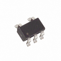
MAX1683EUK+T Maxim Integrated Products, MAX1683EUK+T Datasheet - Page 7

MAX1683EUK+T
Manufacturer Part Number
MAX1683EUK+T
Description
IC VOLT DBLR SW CAP SOT23-5
Manufacturer
Maxim Integrated Products
Type
Switched Capacitor (Charge Pump), Doublerr
Datasheet
1.MAX1682EUK-T.pdf
(9 pages)
Specifications of MAX1683EUK+T
Internal Switch(s)
Yes
Synchronous Rectifier
No
Number Of Outputs
1
Voltage - Output
4 ~ 11 V
Current - Output
45mA
Frequency - Switching
35kHz
Voltage - Input
2 ~ 5.5 V
Operating Temperature
-40°C ~ 85°C
Mounting Type
Surface Mount
Package / Case
SOT-23-5, SC-74A, SOT-25
Power - Output
571mW
Function
Step Up
Output Voltage
4 V to 11 V
Output Current
45 mA
Maximum Operating Temperature
+ 85 C
Minimum Operating Temperature
- 40 C
Mounting Style
SMD/SMT
Lead Free Status / RoHS Status
Lead free / RoHS Compliant
Devices can be cascaded to produce an even larger
voltage (Figure 3). The unloaded output voltage is nom-
inally (n + 1) x V
doublers used. This voltage is reduced by the output
resistance of the first device multiplied by the quiescent
current of the second. The output resistance increases
when devices are cascaded. Using a two-stage dou-
bler as an example, output resistance can be approxi-
mated as R
the output resistance of the first stage and R
output resistance of the second stage. A typical value
for a two-stage voltage doubler is 60Ω (with C1 at 10µF
for MAX1682 and 3.3µF for MAX1683). For n stages
with the same C1 value, R
Figure 3. Cascading Devices
C1
C1+
GND
C1-
OUT
MAX1682
MAX1683
= 2 x R
IN
_______________________________________________________________________________________
, where n is the number of voltage
OUT
IN
C2
OUT1
Switched-Capacitor Voltage Doublers
OUT
C1
INPUT
SUPPLY
VOLTAGE
+ R
= (2
Cascading Devices
C1+
GND
C1-
OUT2
n
MAX1682
MAX1683
- 1) x R
, where R
OUT
IN
OUT1
OUT2
OUTPUT
VOLTAGE
OUT1
.
C2
is the
is
Paralleling multiple MAX1682 or MAX1683s reduces
the output resistance. Each device requires its own
pump capacitor (C1), but the reservoir capacitor (C2)
serves all devices (Figure 4). Increase C2’s value by a
factor of n, where n is the number of parallel devices.
Figure 4 shows the equation for calculating output
resistance.
Good layout is important, primarily for good noise per-
formance. To ensure good layout, mount all compo-
nents as close together as possible, keep traces short
to minimize parasitic inductance and capacitance, and
use a ground plane.
Figure 4. Paralleling Devices
C1
R
OUT
= R
OUT
NUMBER OF DEVICES
C1+
GND
C1-
OF SINGLE DEVICE
MAX1682
MAX1683
OUT
IN
C1
Layout and Grounding
Paralleling Devices
C1+
GND
C1-
MAX1682
MAX1683
OUT
IN
OUTPUT
VOLTAGE
VOLTAGE
SUPPLY
INPUT
C2
7


