MAX15032ATA+T Maxim Integrated Products, MAX15032ATA+T Datasheet - Page 2
MAX15032ATA+T
Manufacturer Part Number
MAX15032ATA+T
Description
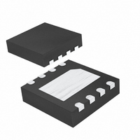
IC DC-DC CONV STEP-UP 8-TDFN
Manufacturer
Maxim Integrated Products
Type
Step-Up (Boost)r
Datasheet
1.MAX15032ATAT.pdf
(10 pages)
Specifications of MAX15032ATA+T
Internal Switch(s)
Yes
Synchronous Rectifier
No
Number Of Outputs
1
Voltage - Output
6.6 ~ 36 V
Current - Output
1A
Frequency - Switching
500kHz
Voltage - Input
2.7 ~ 11 V
Operating Temperature
-40°C ~ 125°C
Mounting Type
Surface Mount
Package / Case
8-TDFN Exposed Pad
Power - Output
1.95W
Lead Free Status / RoHS Status
Lead free / RoHS Compliant


500kHz, 36V Output, 600mW PWM
Step-Up DC-DC Converter
ABSOLUTE MAXIMUM RATINGS
IN to GND ...............................................................-0.3V to +12V
LX to PGND ............................................................-0.3V to +40V
FB to GND ..............................................................-0.3V to +12V
SHDN to GND ..............................................-0.3V to (V
CN to GND .............................................................-0.3V to +12V
CP to GND..............................................................-0.3V to +12V
PGND to GND .......................................................-0.3V to +0.3V
Continuous Power Dissipation (T
ELECTRICAL CHARACTERISTICS
(V
are at T
Note 1: Package thermal resistances were obtained using the method described in JEDEC specification JESD51-7, using a four-
Stresses beyond those listed under “Absolute Maximum Ratings” may cause permanent damage to the device. These are stress ratings only, and functional
operation of the device at these or any other conditions beyond those indicated in the operational sections of the specifications is not implied. Exposure to
absolute maximum rating conditions for extended periods may affect device reliability.
2
SUPPLY VOLTAGE
Supply Voltage Range
Supply Current
Undervoltage Lockout
Undervoltage Lockout Hysteresis
Shutdown Current
LOGIC INPUT (SHDN)
SHDN Input Low Level
SHDN Input High Level
BOOST CONVERTER
Output Voltage Adjustment
Range
Switching Frequency
FB Set Point
FB Input Bias Current
LX Switch On-Resistance
Peak Switch Current Limit
LX Leakage Current
Line Regulation
IN
8-Pin TDFN (derate 24.4mW/°C above +70°C) ......1951.2mW
_______________________________________________________________________________________
= +3.3V, V
A
layer board. For detailed information on package thermal considerations, refer to
= +25°C. See the Typical Operating Circuit .) (Note 2)
PARAMETER
SHDN
= +3.3V, C
A
IN
= +70°C)
= 10µF, PGND = GND = 0V, T
V
SYMBOL
UVLO-HYS
R
I
V
I
LIM_LX
DS_ON
SHDN
UVLO
f
V
V
V
V
I
I
SW
FB
IN
FB
IN
IH
IL
C
CP connected to IN
V
V
V
V
V
V
C
I
CP connected to
IN, I
V
I
LX
LOAD
FB
IN
FB
IN
IN
LX
SHDN
CP
CP
IN
= 100mA
= 3.3V
= 11V
rising
LX
= 1.4V (no switching), C
= 1.4V (no switching), CP = IN,
= 36V
= 10nF
= 10nF,
+ 0.3V)
= 2mA
= 100mA
= 0V
CONDITIONS
A
= T
Junction-to-Case Thermal Resistance (θ
Junction-to-Ambient Thermal Resistance (θ
Operating Temperature Range .........................-40°C to +125°C
Junction Temperature ......................................................+150°C
Storage Temperature Range .............................-65°C to +150°C
Lead Temperature (soldering, 10s) .................................+300°C
V
V
V
V
(Note 1) ........................................................................41°C/W
IN
IN
IN
IN
J
= -40°C to +125°C, unless otherwise noted. Typical values
= 2.9V, V
= 5.5V, V
= V
= V
CP
CP
CP
= 5.5V
= 11V
= 10nF,
CP
CP
= 5.5V
= 10V
www.maxim-ic.com/thermal-tutorial.
V
2.375
1.214
IN
MIN
450
2.7
5.5
2.0
1
+ 1
1.245
TYP
0.42
0.33
0.42
0.33
1.33
0.25
100
500
1.5
2.5
1
JC
) (Note 1) ........8°C/W
JA
)
2.675
1.276
MAX
550
300
5.5
0.5
0.8
1.7
11
36
2
3
1
1
1
1
2
UNITS
kHz
mA
mV
µA
µA
nA
%
Ω
A
V
V
V
V
V
V
Related parts for MAX15032ATA+T
Image
Part Number
Description
Manufacturer
Datasheet
Request
R

Part Number:
Description:
Manufacturer:
Maxim Integrated Products
Datasheet:

Part Number:
Description:
MAX CLIP
Manufacturer:
Aavid Thermalloy
Datasheet:
Part Number:
Description:
MAX7528KCWPMaxim Integrated Products [CMOS Dual 8-Bit Buffered Multiplying DACs]
Manufacturer:
Maxim Integrated Products
Datasheet:
Part Number:
Description:
Single +5V, fully integrated, 1.25Gbps laser diode driver.
Manufacturer:
Maxim Integrated Products
Datasheet:
Part Number:
Description:
Single +5V, fully integrated, 155Mbps laser diode driver.
Manufacturer:
Maxim Integrated Products
Datasheet:
Part Number:
Description:
VRD11/VRD10, K8 Rev F 2/3/4-Phase PWM Controllers with Integrated Dual MOSFET Drivers
Manufacturer:
Maxim Integrated Products
Datasheet:
Part Number:
Description:
Highly Integrated Level 2 SMBus Battery Chargers
Manufacturer:
Maxim Integrated Products
Datasheet:
Part Number:
Description:
Current Monitor and Accumulator with Integrated Sense Resistor; ; Temperature Range: -40°C to +85°C
Manufacturer:
Maxim Integrated Products
Part Number:
Description:
TSSOP 14/A°/RS-485 Transceivers with Integrated 100O/120O Termination Resis
Manufacturer:
Maxim Integrated Products
Part Number:
Description:
TSSOP 14/A°/RS-485 Transceivers with Integrated 100O/120O Termination Resis
Manufacturer:
Maxim Integrated Products
Part Number:
Description:
QFN 16/A°/AC-DC and DC-DC Peak-Current-Mode Converters with Integrated Step
Manufacturer:
Maxim Integrated Products
Part Number:
Description:
TDFN/A/65V, 1A, 600KHZ, SYNCHRONOUS STEP-DOWN REGULATOR WITH INTEGRATED SWI
Manufacturer:
Maxim Integrated Products
Part Number:
Description:
Integrated Temperature Controller f
Manufacturer:
Maxim Integrated Products
Part Number:
Description:
SOT23-6/I°/45MHz to 650MHz, Integrated IF VCOs with Differential Output
Manufacturer:
Maxim Integrated Products
Part Number:
Description:
SOT23-6/I°/45MHz to 650MHz, Integrated IF VCOs with Differential Output
Manufacturer:
Maxim Integrated Products