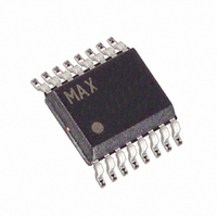
MAX1672EEE Maxim Integrated Products, MAX1672EEE Datasheet - Page 10

MAX1672EEE
Manufacturer Part Number
MAX1672EEE
Description
IC DC/DC CONV STP-UP/DWN 16-QSOP
Manufacturer
Maxim Integrated Products
Type
Step-Down (Buck), Step-Up (Boost)r
Datasheet
1.MAX1672EEE.pdf
(11 pages)
Specifications of MAX1672EEE
Internal Switch(s)
Yes
Synchronous Rectifier
No
Number Of Outputs
1
Voltage - Output
3.3V, 5V, Adj
Current - Output
300mA
Voltage - Input
1.8 ~ 11 V
Operating Temperature
-40°C ~ 85°C
Mounting Type
Surface Mount
Package / Case
16-QSOP
Power - Output
667mW
Output Voltage
1.25 V to 5.5 V
Output Current
300 mA
Input Voltage
1.8 V to 11 V
Supply Current
85 uA
Mounting Style
SMD/SMT
Maximum Operating Temperature
+ 85 C
Minimum Operating Temperature
- 40 C
Lead Free Status / RoHS Status
Contains lead / RoHS non-compliant
Frequency - Switching
-
Other names
Q1162903B
Available stocks
Company
Part Number
Manufacturer
Quantity
Price
Company:
Part Number:
MAX1672EEE
Manufacturer:
MAX
Quantity:
132
Part Number:
MAX1672EEE
Manufacturer:
MAX
Quantity:
20 000
Company:
Part Number:
MAX1672EEE+
Manufacturer:
Maxim
Quantity:
753
Company:
Part Number:
MAX1672EEE+T
Manufacturer:
Maxim
Quantity:
2 500
Company:
Part Number:
MAX1672EEE+T
Manufacturer:
MAXIM
Quantity:
3 415
Part Number:
MAX1672EEE+T
Manufacturer:
MAXIM/美信
Quantity:
20 000
Step-Up/Down DC-DC Converter
in QSOP Package
A single pushbutton switch can be used to turn the
MAX1672 on and off. As shown in Figure 3, ONA is
pulled low and ONB is pulled high when the part is off.
When the momentary switch is pressed, ONB is pulled
low and the regulator turns on. The switch should be on
long enough for the µC to exit reset. The controller
issues a logic high to ONA, which guarantees the part
will stay on regardless of the switch state.
To turn off the regulator, press the switch again. The
controller reads the switch status and pulls ONA low.
When the switch is released, ONB goes high, turning
off the MAX1672.
Thermal overload protection limits total power dissipa-
tion in the MAX1672. When the junction temperature
exceeds T
allowing the MAX1672 to cool. The pass transistor turns
on again after the IC’s junction temperature cools by
20°C, resulting in a pulsed output during thermal over-
load conditions.
Thermal overload protection is designed to protect the
MAX1672 if fault conditions occur. It is not intended to
be used as an operating mode. Prolonged operation in
thermal shutdown mode may reduce the IC’s reliability.
For continual operation, do not exceed the absolute
maximum junction temperature rating T
The MAX1672’s maximum power dissipation in step-
down mode depends on the thermal resistance of the
case and circuit board, the temperature difference
between the die junction and ambient air, and the air
flow rate. The power dissipated in the device is
P = I
maximum power dissipation is as follows:
where (T
the MAX1672 die junction and the surrounding air,
(or
cuit board, copper traces, and other materials to the
surrounding air. The MAX1672’s thermal resistance is
120°C/W. See the Typical Operating Characteristics for
the Maximum Output Current vs. Input Voltage Graph.
10
__________Applications Information
BA
Using a Single, Pushbutton On/Off Switch
Power Dissipation and Operating Region
is the thermal resistance throughout the printed cir-
______________________________________________________________________________________
JC
OUT
) is the thermal resistance of the package, and
J
(V
- T
J
IN
= +150°C, the pass transistor turns off,
A
- V
) is the temperature difference between
P
OUT
MAX
Thermal Overload Protection
) during step-down operation. The
= (T
J
- T
A
)/(
JB
+
J
= +150°C.
BA
)
JB
Proper PC board layout is essential to minimize noise
due to high inductor current levels and fast switching
waveforms. To maximize output power and efficiency
and minimize output ripple voltage and ground noise,
use the following guidelines when designing your
board:
Refer to the MAX1672 EV kit for a suggested PC board
layout.
Figure 3. Momentary Pushbutton On/Off Control
Use a ground plane.
Keep the IC’s GND pin and the ground leads of C1
and C2 (Figure 2) less than 0.2in. (5mm) apart.
Make all connections to the FB and LX pins as short
as possible.
Solder the IC’s GND pin directly to the ground
plane.
1M
1M
ONB
ONA
MAX1672
PS
OUT
Layout Considerations
I/O
I/O
V
DD
C


