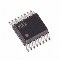
MAX1672EEE+T Maxim Integrated Products, MAX1672EEE+T Datasheet - Page 5

MAX1672EEE+T
Manufacturer Part Number
MAX1672EEE+T
Description
IC DC-DC CONVERT 16-QSOP
Manufacturer
Maxim Integrated Products
Type
Step-Down (Buck), Step-Up (Boost)r
Datasheet
1.MAX1672EEE.pdf
(11 pages)
Specifications of MAX1672EEE+T
Internal Switch(s)
Yes
Synchronous Rectifier
No
Number Of Outputs
1
Voltage - Output
3.3V, 5V, Adj
Current - Output
300mA
Voltage - Input
1.8 ~ 11 V
Operating Temperature
-40°C ~ 85°C
Mounting Type
Surface Mount
Package / Case
16-QSOP
Power - Output
667mW
Lead Free Status / RoHS Status
Lead free / RoHS Compliant
Frequency - Switching
-
Lead Free Status / Rohs Status
Lead free / RoHS Compliant
(T
______________________________________________________________Pin Description
A
PIN
10
11
12
13
14
15
16
= +25°C, unless otherwise noted.)
1
2
3
4
5
6
7
8
9
A: V
B: I
L1
OUT
OUTPUT RIPPLE (HEAVY LOAD)
(500mA/div) (V
= 5V (20mV/div, AC COUPLED)
NAME
PGND
PGND
GND
ONB
ONA
PGO
ILIM
OUT
REF
PGI
3/5
LX
FB
PS
LX
IN
10 s/div
IN
= 2.7V, I
_______________________________________________________________________________________
Inductor Connection to the Drain of the Internal N-Channel Power MOSFET
Power Ground
On Control Input. When ONB = low or ONA = high, the IC is on. Connect ONB to GND for normal operation
(Table 1).
On Control Input. When ONA = low and ONB = high, the IC is off. Connect ONA to PS for normal operation
(Table 1).
Output Voltage Selection Input. Connect to PS for 3.3V output and to GND for 5V output. With V
the state of the 3/5 pin is ignored (Table 2).
Low-Battery Detector Input (1.25V threshold)
Low-Battery Detector Output (open drain). PGO pulls low when V
Inductor-Current-Limit Selection Input. Connect to PS for 0.8A current limit and to GND for 0.5A current limit.
Regulator Output. Drain of internal PFET linear regulator. Bypass with a 4.7µF capacitor to GND.
Feedback Input. For 3.3V or 5V output, connect to GND. For adjustable output, connect to feedback resistor-
divider network. With V
Bootstrapped Power Supply. Output of step-up switch-mode regulator and source of internal PFET linear
regulator. The IC is powered from this pin.
Input Voltage Sense Input. Connect to input supply.
Reference Voltage Output. Bypass with a 0.1µF capacitor to GND.
Analog Ground
Power Ground
Inductor Connection to the Drain of the Internal N-Channel Power MOSFET
OUT
= 250mA)
MAX1672-13
A
B
Step-Up/Down DC-DC Converter
FB
Typical Operating Characteristics (continued)
> 70mV, the state of the 3/5 pin is ignored.
A: V
B: ONB (2V/div) (V
OUT
= (2V/div)
STARTUP DELAY
IN
50 s/div
= 2.7V, R
LOAD
FUNCTION
= 50 )
MAX1672-14
A
B
in QSOP Package
PGI
is greater than 1.25V.
A: V
B: ONB (2V/div) (V
OUT
= (2V/div)
TURN-OFF DELAY
IN
200 s/div
= 2.7V, R
LOAD
= 50 )
FB
MAX1672-15
> 80mV,
A
B
5


