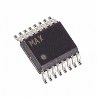
MAX1763EEE Maxim Integrated Products, MAX1763EEE Datasheet - Page 10

MAX1763EEE
Manufacturer Part Number
MAX1763EEE
Description
IC CONV DC/DC STEP UP LN 16QSOP
Manufacturer
Maxim Integrated Products
Type
Step-Up (Boost)r
Datasheet
1.MAX1763EEE.pdf
(16 pages)
Specifications of MAX1763EEE
Internal Switch(s)
Yes
Synchronous Rectifier
Yes
Number Of Outputs
1
Voltage - Output
3.3V, 2.5 ~ 5.5 V
Current - Output
1.5A
Frequency - Switching
1MHz
Voltage - Input
0.7 ~ 5.5 V
Operating Temperature
-40°C ~ 85°C
Mounting Type
Surface Mount
Package / Case
16-QSOP
Power - Output
667mW
Output Voltage
3.3 V
Output Current
1.5 A
Input Voltage
0.7 V to 5.5 V
Supply Current
2.5 mA
Switching Frequency
1200 MHz
Mounting Style
SMD/SMT
Maximum Operating Temperature
+ 85 C
Minimum Operating Temperature
- 40 C
Lead Free Status / RoHS Status
Contains lead / RoHS non-compliant
Available stocks
Company
Part Number
Manufacturer
Quantity
Price
Part Number:
MAX1763EEE
Manufacturer:
MAXIM/美信
Quantity:
20 000
block can also function as a voltage-monitoring com-
parator. The MAX1763 is available in a 16-pin QSOP
package or a 1.5W 16-pin TSSOP-EP package for high-
temperature or high-dissipation applications.
During DC-DC converter operation, the internal N-chan-
nel MOSFET switch turns on for the first part of each
cycle, allowing current to ramp up in the inductor and
store energy in a magnetic field. During the second
part of each cycle, the MOSFET turns off and inductor
current flows through the synchronous rectifier to the
output filter capacitor and the load. As the energy
stored in the inductor is depleted, the current ramps
down and the synchronous rectifier turns off, the N-
channel FET turns on, and the cycle repeats. At light
loads, depending on the CLK/SEL pin setting, output
voltage is regulated using either PWM or by switching
only as needed to service the load (Table 2).
Pulling CLK/SEL low selects the MAX1763’s normal
operating mode. In this mode, the device operates in
PWM when driving medium to heavy loads, and at light
loads only, switches as needed. This optimizes efficien-
cy over the widest range of load conditions. In normal
operation mode, the output voltage regulates 1% higher
than in forced-PWM mode. See Efficiency vs. Load
Current in the Typical Operating Characteristics section.
When CLK/SEL is high, the MAX1763 operates in a low-
noise forced-PWM mode. During forced-PWM opera-
tion, the MAX1763 switches at a constant frequency
(1MHz) and modulates the MOSFET switch pulse width
to control the power transferred per cycle and regulate
the output voltage. Switching harmonics generated by
fixed-frequency operation are consistent and easily fil-
tered. See the Noise Spectrum plot in the Typical
Operating Characteristics.
1.5A, Low-Noise, 1MHz, Step-Up
DC-DC Converter
Table 2. Selecting the Operating Mode
10
External clock
500kHz to 1.2MHz
______________________________________________________________________________________
CLK/SEL
0
1
Normal
operation
Forced PWM
S ynchr oni zed
P WM
MODE
Step-Up Converter
Forced-PWM Operation
Normal Operation
High efficiency at all
loads. Fixed
frequency at all but
light loads.
Low noise, fixed
frequency at all loads.
Low noise, fixed
frequency at all loads.
FEATURES
In a variation of forced-PWM mode, the MAX1763 can
be synchronized to an external frequency by applying
a clock signal to CLK/SEL. This allows the user to
choose an operating frequency (from 500kHz to
1.2MHz) to avoid interference in sensitive applications.
For the most noise-sensitive applications, limit the
external synchronization signal duty cycle to less than
10% or greater than 90%. This eliminates the possibility
that noise from the power switching will coincide with
the synchronization signal. If the synchronization signal
edge falls on the power switching edge, a slight fre-
quency jitter may occur.
The MAX1763 features an internal 130mΩ P-channel syn-
chronous rectifier to enhance efficiency. Synchronous
rectification provides a 5% efficiency improvement over
similar boost regulators that rely on diode rectifiers. In
PWM mode, the synchronous rectifier is turned on during
the second half of each switching cycle. In low-power
mode, an internal comparator turns on the synchronous
rectifier when the voltage at LX exceeds the boost regula-
tor output and turns it off when the inductor current drops
below 120mA. When setting output voltages greater than
4V, an external 0.5A Schottky diode must be connected
in parallel with the on-chip synchronous rectifier.
The MAX1763 uses a CMOS low-voltage startup oscil-
lator for a 1.1V guaranteed minimum startup input volt-
age. At startup, the low-voltage oscillator switches the
N-channel MOSFET until the output voltage reaches
2.15V. Above this level, the normal feedback and con-
trol circuitry take over. Once the device is in regulation,
it can operate down to 0.7V input because internal
power for the IC is derived from the output through the
OUT pin. Do not apply full system load until the output
exceeds 2.3V.
ONA and ONB turn the MAX1763 on or off. When ONA =
1 or ONB = 0, the device is on. When ONA = 0 and
ONB = 1, the device is off (Table 3). Logic high ON
control can be implemented by connecting ONB high
and using ONA for the control input. Momentary one-
pushbutton ON/OFF control is described in the
Applications Information section. Both ONA and ONB
have approximately (0.15
The MAX1763 has an internal 1.250V reference.
Connect a 0.22µF ceramic bypass capacitor to GND
Low-Voltage Startup Oscillator
Synchronized-PWM Operation
✕
Synchronous Rectifier
V
Shutdown, ONA,
OUT
)V of hysteresis.
Reference
ONB


