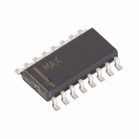
MAX797CSE+T Maxim Integrated Products, MAX797CSE+T Datasheet - Page 9

MAX797CSE+T
Manufacturer Part Number
MAX797CSE+T
Description
IC CNTRLR STEP DOWN 16-SOIC
Manufacturer
Maxim Integrated Products
Type
Step-Down (Buck)r
Datasheet
1.MAX797CSE.pdf
(32 pages)
Specifications of MAX797CSE+T
Internal Switch(s)
No
Synchronous Rectifier
Yes
Number Of Outputs
2
Voltage - Output
3.3V, 5V, Adj
Current - Output
10A
Frequency - Switching
150kHz, 300kHz
Voltage - Input
4.5 ~ 30 V
Operating Temperature
0°C ~ 70°C
Mounting Type
Surface Mount
Package / Case
16-SOIC (3.9mm Width)
Power - Output
696mW
Lead Free Status / RoHS Status
Lead free / RoHS Compliant
Dual Mode is a trademark of Maxim Integrated Products.
______________________________________________________________Pin Description
PIN
10
11
12
13
14
15
16
1
2
3
4
5
6
7
8
9
(MAX796/
(MAX797)
MAX799)
SECFB
NAME
PGND
SHDN
SYNC
GND
SKIP
CSH
CSL
REF
BST
DH
SS
FB
V+
VL
DL
LX
_______________________________________________________________________________________
• MAX796: SECFB regulates at VSECFB = 2.505V. Tie to VL if not used.
• MAX799: SECFB regulates at VSECFB = 0V. Tie to a negative voltage through a high-value current-limit-
• Connect to GND for 3.3V operation.
• Connect to VL for 5V operation.
• Connect FB to a resistor divider for adjustable mode. FB can be driven with +5V rail-to-rail logic in order to
Soft-Start timing capacitor connection. Ramp time to full current limit is approximately 1ms/nF.
Secondary winding Feedback input. Normally connected to a resistor divider from an auxiliary output.
Don’t leave SECFB unconnected.
Disables pulse-skipping mode when high. Connect to GND for normal use. Don’t leave SKIP unconnected.
With SKIP grounded, the device will automatically change from pulse-skipping operation to full PWM opera-
tion when the load current exceeds approximately 30% of maximum. (See Table 3.)
Reference voltage output. Bypass to GND with 0.33µF minimum.
Low-noise analog Ground and feedback reference point.
Oscillator Synchronization and frequency select. Tie to GND or VL for 150kHz operation; tie to REF for
300kHz operation. A high-to-low transition begins a new cycle. Drive SYNC with 0V to 5V logic levels (see the
Electrical Characteristics table for V
guaranteed.
Shutdown control input, active low. Logic threshold is set at approximately 1V (V
MOSFET). Tie SHDN to V+ for automatic start-up.
Feedback input. Regulates at FB = REF (approximately 2.505V) in adjustable mode. FB is a Dual-Mode
input that also selects the fixed output voltage settings as follows:
Current-Sense input, High side. Current-limit level is 100mV referred to CSL.
Current-Sense input, Low side. Also serves as the feedback input in fixed-output modes.
Battery voltage input (4.5V to 30V). Bypass V+ to PGND close to the IC with a 0.1µF capacitor. Connects to a
linear regulator that powers VL.
5V Internal linear-regulator output. VL is also the supply voltage rail for the chip. VL is switched to the output
voltage via CSL (V
supply up to 5mA for external loads.
Power Ground.
Low-side gate-drive output. Normally drives the synchronous-rectifier MOSFET. Swings 0V to VL.
Boost capacitor connection for high-side gate drive (0.1µF).
Switching node (inductor) connection. Can swing 2V below ground without hazard.
High-side gate-drive output. Normally drives the main buck switch. DH is a floating driver output that swings
from LX to BST, riding on the LX switching-node voltage.
ing resistor (I
change the output voltage under system control.
Synchronous Rectifier for CPU Power
MAX
CSL
= 100µA) if not used.
> 4.5V) for automatic bootstrapping. Bypass to GND with 4.7µF. VL can
Step-Down Controllers with
IH
and V
IL
specifications). SYNC capture range is 190kHz to 340kHz
FUNCTION
TH
of an internal N-channel
TM
9


