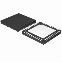
MAX8686ETL+T Maxim Integrated Products, MAX8686ETL+T Datasheet - Page 13

MAX8686ETL+T
Manufacturer Part Number
MAX8686ETL+T
Description
IC BUCK SYNC ADJ 25A 40TQFN
Manufacturer
Maxim Integrated Products
Type
Step-Down (Buck)r
Datasheet
1.MAX8686ETL.pdf
(23 pages)
Specifications of MAX8686ETL+T
Internal Switch(s)
Yes
Synchronous Rectifier
Yes
Number Of Outputs
1
Voltage - Output
0.7 ~ 5.5 V
Current - Output
25A
Frequency - Switching
300kHz ~ 1MHz
Voltage - Input
4.5 ~ 20 V
Operating Temperature
-40°C ~ 85°C
Mounting Type
Surface Mount
Package / Case
40-TQFN Exposed Pad
Power - Output
4W
Lead Free Status / RoHS Status
Lead free / RoHS Compliant
The current-limit threshold is set by a resistor between
ILIM and GND. Under soft-overload conditions, when
the peak inductor current exceeds the selected current
limit, the high-side MOSFET is turned off immediately
and the low-side MOSFET is turned on and remains on
to let the inductor current ramp down until the next
clock cycle. The converter does not stop switching and
the output voltage regulation is not guaranteed. Under
severe-overload or short-circuit conditions, the foldback
and hiccup current limit is simultaneously activated to
reduce power dissipation in the inductor, internal power
MOSFETs, and the upstream power source. Thus, the
circuit can withstand short-circuit conditions continu-
ously without causing overheating of any component. If
the device experiences a persistent overload condition,
the device will autoretry with a soft-start. The converter
will resume normal operation after the overload condi-
tion is removed.
The current-limit input is also used to communicate faults
between the devices in a multiphase configuration. With
any fault on the slave or master device (such as UVLO or
overtemperature), the ILIM input is pulled low, which
causes the other devices to turn off both MOSFETs.
Accurate current sharing is required in a multiphase con-
verter to prevent some phases from overheating during
soft-start, steady-state, and load transient. For a convert-
er with current-mode control, the current is proportional
to the error-amplifier output in the voltage feedback loop.
The error-amplifier output (COMP) of the master is con-
nected to the current comparator input of all slave
devices. The current-sharing accuracy is determined by
the tolerances of the inductance and inductor DCR, the
input offset voltage, the gain of the current-sense ampli-
fiers, and the slope compensation circuits.
The peak current-mode control is an open-loop current-
sharing scheme, and therefore no compensation for
current sharing is needed and no stability issue exists.
The MAX8686 has an adjustable internal oscillator that
can be set to any frequency from 300kHz to 1MHz. To set
the switching frequency, connect a capacitor from the
FREQ to GFREQ (see Setting the Switching Frequency
section).
A triangle ramp from 0 to AVL/2 is generated across
FREQ capacitor. In a multiphase application, the
capacitor needs to be connected to the master device.
DC-DC Converter Delivers Up to 25A Per Phase
______________________________________________________________________________________
Switching Frequency and
Ramp Generation (FREQ)
Current-Limit Circuit
Current Sharing
Single/Multiphase, Step-Down,
The FREQ inputs of the master and slave devices need
to be connected together. FREQ is internally pulled
down to GFREQ during shutdown.
For single-phase or master device operation, the
PHASE/REFO can be used as a reference for the con-
verter output voltage (see the Reference Output
(PHASE/REFO)/Reference Input (REFIN) section). For
multiphase operation, connect the PHASE/REFO of
each slave device to the center tap of the resistor-
divider from AVL of the master to GND. The resistor val-
ues are selected to set delay time between phases (see
the Calculating the Phase Voltage section). The PWM
clock cycle of slave devices starts 60ns after the rising
edge of the voltage at FREQ crosses the voltage at
PHASE/REFO. The PWM clock cycle of the master
device starts at the beginning of the ramp.
For single-phase or master operation, connect RS+ to
the sense point at the load and RS- to the GND sense
point of the load. The connections should be at the out-
put regulation point to eliminate the voltage-sense error
caused by voltage drop between the device and load.
The RS+ and RS- traces should be laid out in parallel to
reduce noise coupling. A common-mode filter to each
sense trace should be added if further noise reduction
is needed.
For an output voltage higher than 3.3V, tie
PHASE/REFO to REFIN and use a resistor-divider from
the output regulation point to the remote sense inputs
(RS+, RS-), as shown in Figure 1b.
For multiphase operation, connect RS+ and RS- to AVL
(slave) to select the slave mode.
Figure 1b. Output Voltage Above 3.3V
Phase Selection Input (PHASE/REFO)
MAX8686
Remote Sense Input (RS+, RS-)
PHASE/REFO
REFIN
RS+
RS-
V
OUT
R1
R2
LOAD
13


