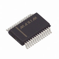
MAX1631EAI Maxim Integrated Products, MAX1631EAI Datasheet - Page 20

MAX1631EAI
Manufacturer Part Number
MAX1631EAI
Description
IC PS CTRLR FOR NOTEBOOKS 28SSOP
Manufacturer
Maxim Integrated Products
Type
Step-Down (Buck)r
Datasheet
1.MAX1634CAI.pdf
(29 pages)
Specifications of MAX1631EAI
Internal Switch(s)
No
Synchronous Rectifier
Yes
Number Of Outputs
2
Voltage - Output
3.3V, 5V, Adj
Current - Output
4A
Frequency - Switching
200kHz, 300kHz
Voltage - Input
4.2 ~ 30 V
Operating Temperature
-40°C ~ 85°C
Mounting Type
Surface Mount
Package / Case
28-SSOP
Power - Output
762mW
Output Voltage
2.5 V to 5.5 V, 3.3 V, 5 V
Input Voltage
4.2 V to 30 V
Mounting Style
SMD/SMT
Maximum Operating Temperature
+ 85 C
Minimum Operating Temperature
- 40 C
Case
SSOP
Dc
98+
Lead Free Status / RoHS Status
Contains lead / RoHS non-compliant
Available stocks
Company
Part Number
Manufacturer
Quantity
Price
Part Number:
MAX1631EAI
Manufacturer:
MAXIM/美信
Quantity:
20 000
Company:
Part Number:
MAX1631EAI+T
Manufacturer:
Maxim
Quantity:
6 066
Part Number:
MAX1631EAI-T
Manufacturer:
MAXIM/美信
Quantity:
20 000
Multi-Output, Low-Noise Power-Supply
Controllers for Notebook Computers
systems can multiply the R
without hurting stability or transient response.
The output voltage ripple is usually dominated by the
filter capacitor’s ESR, and can be approximated as
I
full equation for ripple in continuous-conduction mode
is V
C
discontinuous, with high peaks and widely spaced
pulses, so the noise can actually be higher at light load
(compared to full load). In Idle Mode, calculate the out-
put ripple as follows:
Buck-plus-flyback applications, sometimes called “cou-
pled-inductor” topologies, need a transformer to gener-
ate multiple output voltages. Performing the basic
electrical design is a simple task of calculating turns
ratios and adding the power delivered to the secondary
to calculate the current-sense resistor and primary
inductance. However, extremes of low input-output dif-
ferentials, widely different output loading levels, and
high turns ratios can complicate the design due to par-
asitic transformer parameters such as interwinding
capacitance, secondary resistance, and leakage
inductance. For examples of what is possible with real-
world transformers, see the Maximum Secondary
Current vs. Input Voltage graph in the Typical
Operating Characteristics section.
Power from the main and secondary outputs is com-
bined to get an equivalent current referred to the main
output voltage (see the Inductor Value section for para-
meter definitions). Set the current-sense resistor resis-
tor value at 80mV / I
P
I
20
RIPPLE
TOTAL
V
TOTAL
OUT
NOISE(p-p)
NOISE (p-p)
L(primary) =
______________________________________________________________________________________
Turns Ratio N =
)]. In Idle Mode, the inductor current becomes
= P
x R
= The sum of the output power from all outputs
rent referred to V
ESR
TOTAL
=
. There is also a capacitive term, so the
0.02 x R
0.0003 x Lx 1 / V
= I
R
/ V
V
SENSE
TOTAL
(for Auxiliary Outputs Only)
IN(MAX)
RIPPLE
OUT
V
OUT
V
OUT(MIN)
ESR
.
= The equivalent output cur-
(R
(V
OUT
ESR
SENSE
IN(MAX)
x f x I
x [R
[
V
+
Transformer Design
SEC
value by a factor of 1.5
+ V
OUT
ESR
TOTAL
) x C
2
+ V
RECT
- V
+
+ 1/(2 x π x f x
OUT
1 / (V - V
FWD
OUT
x LIR
+ V
)
IN
SENSE
OUT
)
]
where: V
In positive-output applications, the transformer sec-
ondary return is often referred to the main output volt-
age, rather than to ground, to reduce the needed turns
ratio. In this case, the main output voltage must first be
subtracted from the secondary voltage to obtain V
The high-current N-channel MOSFETs must be logic-level
types with guaranteed on-resistance specifications at
V
ter (i.e., 2V max rather than 3V max). Drain-source break-
down voltage ratings must at least equal the maximum
input voltage, preferably with a 20% derating factor. The
best MOSFETs will have the lowest on-resistance per
nanocoulomb of gate charge. Multiplying R
provides a good figure for comparing various MOSFETs.
Newer MOSFET process technologies with dense cell
structures generally perform best. The internal gate
drivers tolerate >100nC total gate charge, but 70nC is a
more practical upper limit to maintain best switching
times.
In high-current applications, MOSFET package power
dissipation often becomes a dominant design factor.
I
both high-side and low-side MOSFETs. I
distributed between Q1 and Q2 according to duty fac-
tor (see the following equations). Generally, switching
losses affect only the upper MOSFET, since the
Schottky rectifier clamps the switching node in most
cases before the synchronous rectifier turns on. Gate-
charge losses are dissipated by the driver and don’t
heat the MOSFET. Calculate the temperature rise
according to package thermal-resistance specifications
to ensure that both MOSFETs are within their maximum
junction temperature at high ambient temperature. The
worst-case dissipation for the high-side MOSFET
occurs at both extremes of input voltage, and the
worst-case dissipation for the low-side MOSFET occurs
at maximum input voltage.
2
GS
R power losses are the greatest heat contributor for
= 4.5V. Lower gate threshold specifications are bet-
V
V
V
V
SEC
FWD
OUT(MIN)
RECT
SENSE
= the minimum required rectified sec-
= the forward drop across the secondary
= the on-state voltage drop across the
rectifier
= the voltage drop across the sense
ondary output voltage
synchronous rectifier MOSFET
Selecting Other Components
resistor
= the minimum value of the main
output voltage (from the Electrical
Characteristics)
MOSFET Switches
2
R losses are
DS(ON)
SEC
x Q
.
G


