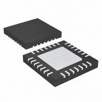
MAX5073ATI+T Maxim Integrated Products, MAX5073ATI+T Datasheet - Page 22

MAX5073ATI+T
Manufacturer Part Number
MAX5073ATI+T
Description
IC CONV BUCK/BOOST 28-TQFN
Manufacturer
Maxim Integrated Products
Type
Step-Down (Buck), Step-Up (Boost)r
Datasheet
1.MAX5073ETI.pdf
(25 pages)
Specifications of MAX5073ATI+T
Internal Switch(s)
Yes
Synchronous Rectifier
No
Number Of Outputs
2
Voltage - Output
0.8 ~ 28 V
Current - Output
1A, 2A
Frequency - Switching
200kHz ~ 2.2MHz
Voltage - Input
4.5 ~ 23 V
Operating Temperature
-40°C ~ 85°C
Mounting Type
Surface Mount
Package / Case
28-TQFN Exposed Pad
Power - Output
2.76W
Lead Free Status / RoHS Status
Lead free / RoHS Compliant
2.2MHz, Dual-Output Buck or Boost Converter
with Internal Power MOSFETs
3) Calculate C
where ω
4) Place a pole
5) Place the second zero
6) Place the second pole
In applications where the MAX5073 are subject to noisy
environments, adjust the controller’s compensation to
improve the system’s noise immunity. In particular,
high-frequency noise coupled into the feedback loop
causes jittery duty cycles. One solution is to lower the
crossover frequency (see the Compensation section).
Careful PC board layout is critical to achieve low
switching losses and clean, stable operation. This is
especially true for dual converters where one channel
can affect the other. Refer to the MAX5073 EV kit data
sheet for a specific layout example. Use a multilayer
board whenever possible for better noise immunity.
Follow these guidelines for good PC board layout:
1) For SGND, use a large copper plane under the IC
22
the switching frequency.
and solder it to the exposed paddle. To effectively
use this copper area as a heat exchanger between
the PC board and ambient, expose this copper area
______________________________________________________________________________________
C
= 2π f
C
C
I
CF
=
I
for a target crossover frequency, f
R
V
C
=
(
R
f
OSC
I
P
1
(
1
=
2
=
PC Board Layout Guidelines
π
=
2π
2
⎡
⎣ ⎢
Improving Noise Immunity
×
(
π
2
1
×
0 5
π
−
×
f
.
ω
ZERO
D
×
f
C F IN
(
LC
1
(f
×
f
)
R
Z
1
2
R V
P
2
f
I
2
SW
1
+
×
×
C
,
=
R
=
ω
C
F
C
HP
×
2
C
I
2
I
π
R
2
)
π
−
L C
F
×
at f
×
×
R
O O
C
×
R
I
R
1
I
ZERO,RHP
1
C
F
1
×
F
⎤
⎦ ⎥
×
)
C
−
C
I
1
)
CF
at f
.
C
at 1/2
LC
:
.
2) Isolate the power components and high-current
3) Keep the high-current paths short, especially at the
4) Connect SGND and PGND together close to the IC
5) Keep the power traces and load connections short.
6) Ensure that the feedback connection to C
7) Route high-speed switching nodes (BST_/VDD_,
on the top and bottom side of the PC board. Do not
make a direct connection from the exposed pad
copper plane to SGND (pin 25) underneath the IC.
path from the sensitive analog circuitry.
ground terminals. This practice is essential for sta-
ble, jitter-free operation.
at the ground terminals of VL and V+ bypass capac-
itors. Do not connect them together anywhere else.
This practice is essential for high efficiency. Use
thick copper PC boards (2oz vs. 1oz) to enhance
full-load efficiency.
short and direct.
SOURCE_) away from the sensitive analog areas
(BYPASS, COMP_, and FB_). Use the internal PC
board layer for SGND as EMI shields to keep radiat-
ed noise away from the IC, feedback dividers, and
analog bypass capacitors.
OUT
is


