MAX15017BATX+ Maxim Integrated Products, MAX15017BATX+ Datasheet - Page 16
MAX15017BATX+
Manufacturer Part Number
MAX15017BATX+
Description
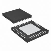
IC DC/DC CONV 1A 36-TQFN-EP
Manufacturer
Maxim Integrated Products
Type
Step-Down (Buck)r
Datasheet
1.MAX15017AATX.pdf
(26 pages)
Specifications of MAX15017BATX+
Internal Switch(s)
Yes
Synchronous Rectifier
Yes
Number Of Outputs
2
Voltage - Output
1.26 ~ 32 V
Current - Output
1A
Frequency - Switching
135kHz ~ 500kHz
Voltage - Input
7.5 ~ 40 V
Operating Temperature
-40°C ~ 125°C
Mounting Type
Surface Mount
Package / Case
36-TQFN Exposed Pad
Power - Output
2.1W
Lead Free Status / RoHS Status
Lead free / RoHS Compliant


1A, 4.5V to 40V Input Buck Converters with
50mA Auxiliary LDO Regulators
SS is the 1.235V reference bypass connection for the
MAX15014–MAX15017 and also controls the soft-start
period. At startup, after input voltage is applied at IN_SW,
IN_LDO and the UVLO thresholds are reached, the
device enters soft-start. During soft-start, 14µA is sourced
into the capacitor (C
causing the reference voltage to ramp up slowly. When
V
the soft-start time (t
where V
I
onds and C
The MAX15015/MAX15016 feature an internal charge
pump to enhance the turn-on of the internal MOSFET,
allowing for operation with input voltages down to 4.5V.
Connect a flying capacitor (C
boost diode from C+ to BST, as well as a bootstrap
capacitor (C
gate drive voltage for the high-side n-channel DMOS
switch. During the on-time, the flying capacitor is
charged to V
minal of the flying capacitor (C+) is pumped to two times
V
twice the regulator voltage across the high-side DMOS
driver. Use a ceramic capacitor of at least 0.1µF for
C
DVREG is the supply input for the internal high-side
MOSFET driver. The power for DVREG is derived from
the output of the internal regulator (REG). Connect
DVREG to REG externally. To filter the switching noise,
the use of an RC filter (1Ω and 0.47µF) from REG to
DVREG is recommended. In the MAX15015/MAX15016,
the high-side drive supply is generated using the inter-
nal charge pump along with the bootstrap diode and
capacitor. In the MAX15014/MAX15017, the high-side
MOSFET driver supply is generated using only the boot-
strap diode and capacitor.
The output of the internal error amplifier (COMP) is avail-
able for frequency compensation (see the Compensation
Design section). The inverting input is FB, the noninverting
input SS, and the output COMP. The error amplifier has an
16
SS
SS
DVREG
BST
= soft-start current = 14 x 10
reaches 1.244V, the output becomes fully active. Set
______________________________________________________________________________________
and C
SS
and charge is dumped onto C
= soft-start reference voltage = 1.235V (typ),
SS
F
BST
DVREG
located as close as possible to the device.
is in Farads.
) between BST and LX to provide the
Soft-Start and Reference (SS)
SS
t
SS
. During the off-time, the positive ter-
Gate Drive Supply (DVREG)
) using following equation:
SS
=
) connected from SS to SGND
V
SS
(MAX15015/MAX15016)
I
Internal Charge Pump
SS
×
C
F
) between C+ and C-, a
SS
-6
A (typ), t
Error Amplifier
BST
SS
to provide
is in sec-
80dB open-loop gain and a 1.8MHz GBW product. See
the Typical Operating Characteristics for the Gain and
Phase vs. Frequency graph.
With SYNC connected to SGND, the MAX15014–
MAX15017 use their internal oscillator and switch at a
fixed frequency of 135kHz and 500kHz. The MAX15014/
MAX15016 are the 135kHz options and MAX15015/
MAX15017 are the 500kHz options. For external syn-
chronization, drive SYNC with an external clock from
400kHz to 600kHz (MAX15015/MAX15017) or 100kHz
to 200kHz (MAX15014/MAX15016). When driven with
an external clock, the device synchronizes to the rising
edge of SYNC.
An internal ramp generator clocked by the internal
oscillator is compared against the output of the error
amplifier to generate the PWM signal. The maximum
amplitude of the ramp (V
compensate for input voltage and oscillator frequency
changes. This causes the V
constant 10V/V across the input voltage range of 4.5V to
40V (MAX15015/MAX15016) or 7.5V to 40V (MAX15014/
MAX15017) and the SYNC frequency range of 400kHz
to 600kHz (MAX15015/MAX15017) or 100kHz to 200kHz
(MAX15014/MAX15016).
The MAX15014–MAX15017 protect against an output
short circuit by utilizing hiccup-mode protection. In hic-
cup mode, a series of sequential cycle-by-cycle
current-limit events cause the part to shut down and
restart with a soft-start sequence. This allows the
device to operate with a continuous output short circuit.
During normal operation, the current is monitored at the
drain of the internal power MOSFET. When the current
limit is exceeded, the internal power MOSFET turns off
until the next on-cycle and a counter increments. If the
counter counts seven consecutive current-limit events,
the device discharges the soft-start capacitor and
shuts down for 512 clock periods before restarting with
a soft-start sequence. Each time the power MOSFET
turns on and the device does not exceed the current
limit, the counter is reset.
The LDO regulator operates over an input voltage from
5V to 40V, and can be enabled independently of the
DC-DC converter section. Its quiescent current is as
low as 47µA with a load current of 100µA. All devices
Oscillator/Synchronization Input (SYNC)
PWM Comparator/Voltage Feed-Forward
Output Short-Circuit Protection
RAMP
) automatically adjusts to
IN_SW
LDO Regulator
(Hiccup Mode)
/ V
RAMP
to be a
Related parts for MAX15017BATX+
Image
Part Number
Description
Manufacturer
Datasheet
Request
R

Part Number:
Description:
Highly Integrated Linear Battery Charger with Thermal Regulation for Portable Applications
Manufacturer:
Maxim Integrated Products
Datasheet:

Part Number:
Description:
MAX CLIP
Manufacturer:
Aavid Thermalloy
Datasheet:
Part Number:
Description:
MAX7528KCWPMaxim Integrated Products [CMOS Dual 8-Bit Buffered Multiplying DACs]
Manufacturer:
Maxim Integrated Products
Datasheet:
Part Number:
Description:
Single +5V, fully integrated, 1.25Gbps laser diode driver.
Manufacturer:
Maxim Integrated Products
Datasheet:
Part Number:
Description:
Single +5V, fully integrated, 155Mbps laser diode driver.
Manufacturer:
Maxim Integrated Products
Datasheet:
Part Number:
Description:
VRD11/VRD10, K8 Rev F 2/3/4-Phase PWM Controllers with Integrated Dual MOSFET Drivers
Manufacturer:
Maxim Integrated Products
Datasheet:
Part Number:
Description:
Highly Integrated Level 2 SMBus Battery Chargers
Manufacturer:
Maxim Integrated Products
Datasheet:
Part Number:
Description:
Current Monitor and Accumulator with Integrated Sense Resistor; ; Temperature Range: -40°C to +85°C
Manufacturer:
Maxim Integrated Products
Part Number:
Description:
TSSOP 14/A°/RS-485 Transceivers with Integrated 100O/120O Termination Resis
Manufacturer:
Maxim Integrated Products
Part Number:
Description:
TSSOP 14/A°/RS-485 Transceivers with Integrated 100O/120O Termination Resis
Manufacturer:
Maxim Integrated Products
Part Number:
Description:
QFN 16/A°/AC-DC and DC-DC Peak-Current-Mode Converters with Integrated Step
Manufacturer:
Maxim Integrated Products
Part Number:
Description:
TDFN/A/65V, 1A, 600KHZ, SYNCHRONOUS STEP-DOWN REGULATOR WITH INTEGRATED SWI
Manufacturer:
Maxim Integrated Products
Part Number:
Description:
Integrated Temperature Controller f
Manufacturer:
Maxim Integrated Products
Part Number:
Description:
SOT23-6/I°/45MHz to 650MHz, Integrated IF VCOs with Differential Output
Manufacturer:
Maxim Integrated Products
Part Number:
Description:
SOT23-6/I°/45MHz to 650MHz, Integrated IF VCOs with Differential Output
Manufacturer:
Maxim Integrated Products