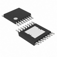
MAX1765EUE+ Maxim Integrated Products, MAX1765EUE+ Datasheet - Page 9

MAX1765EUE+
Manufacturer Part Number
MAX1765EUE+
Description
IC DC-DC CONV 800MA LN 16TSSOP
Manufacturer
Maxim Integrated Products
Type
Step-Up (Boost)r
Datasheet
1.MAX1765EEE.pdf
(19 pages)
Specifications of MAX1765EUE+
Internal Switch(s)
Yes
Synchronous Rectifier
Yes
Number Of Outputs
2
Voltage - Output
2.5 ~ 5.5 V
Current - Output
800mA
Frequency - Switching
1MHz
Voltage - Input
Adj down to 0.7V
Operating Temperature
-40°C ~ 85°C
Mounting Type
Surface Mount
Package / Case
16-TSSOP Exposed Pad, 16-eTSSOP, 16-HTSSOP
Power - Output
1.5W
Output Voltage
2.5 V to 5.5 V
Output Current
800 mA
Input Voltage
0.7 V to 5.5 V
Supply Current
100 uA
Switching Frequency
1200 MHz
Mounting Style
SMD/SMT
Maximum Operating Temperature
+ 85 C
Minimum Operating Temperature
- 40 C
Lead Free Status / RoHS Status
Lead free / RoHS Compliant
C
A
B
(T
(V
A: LX NODE, 5V/div
B: INDUCTOR CURRENT, 200mA/div, AC-COUPLED
C: OUTPUT RIPPLE, 20mV/div, AC-COUPLED
A
LIGHT-LOAD SWITCHING WAVEFORMS
IN
PIN
1
2
3
4
5
6
7
8
= +25°C, unless otherwise noted.)
= +2.4V, V
800mA, Low-Noise, Step-Up DC-DC Converter
OUT
CLK/SEL
500ns/div
NAME
GND
ONA
ISET
OUT
= +3.3V, I
FBL
REF
FB
_______________________________________________________________________________________
OUT
MAX1765 toc17
= 10mA)
Low-Dropout Linear Regulator Dual-Mode Feedback Input. Connect FBL to ground for 2.85V
nominal output voltage. Connect FBL to a resistor-divider from OUTL to ground for an adjustable
output voltage. FBL regulates to 1.25V.
Set N-Channel Current Limit. For maximum current limit, connect ISET to REF. To reduce current
limit, use a resistor-divider from REF to GND. If soft-start is desired, a capacitor can be added from
ISET to GND. When ONA = LO and ONB = HI or V
switchable resistor discharges ISET to GND.
1.25V Reference Output. Connect a 0.22µF bypass capacitor to GND; 50µA of external load current
is allowed. The reference is enabled if ONA = HI, ONB = LO, or ONL = HI.
Ground. Connect to PGND with short trace.
Boost Converter Feedback Input. Connect a resistor-divider between OUT and GND to set the
output voltage in the range of 2.5V to 5V. In track mode, FB is disabled after OUTL is in regulation.
Boost Converter IC power is derived from OUT. Connect OUT to POUT through a 4.7Ω resistor and
bypass to GND with a 0.68µF capacitor.
ON Input. When high, the DC-DC is operational (Table 2).
CLOCK Input for the DC-DC Converter. Also serves to program operating mode of switch as follows:
CLK/SEL = LOW: Normal mode. Operates at a fixed frequency, automatically switching to low-
power (SKIP) mode when the load is minimized.
CLK/SEL = HI: Forced PWM mode. Operates in low-noise, constant-frequency mode at all loads.
CLK/SEL = Clocked: Synchronized forced PWM mode. The internal oscillator is synchronized to an
external clock in the 500kHz to 1200kHz frequency range.
450
350
250
150
50
0
0.1
Typical Operating Characteristics (continued)
I
V
LDO
LINEAR-REGULATOR OUTPUT NOISE
with 500mA Linear Regulator
LDO
= 200mA
= 2.85V
FREQUENCY (MHz)
1
FUNCTION
REF
10
< 80% of nominal value, an on-chip 100kΩ
1.4
1.2
1.0
0.8
0.6
0.4
0.2
0
0
V
SWITCH CURRENT LIMIT vs. V
OUT
0.2
= +3.3
Pin Description
0.4
0.6
V
ISET
(V)
0.8
1.0
1.2
ISET
1.4
9


