MAX1703ESE+ Maxim Integrated Products, MAX1703ESE+ Datasheet - Page 11

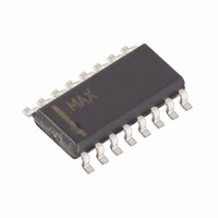
MAX1703ESE+
Manufacturer Part Number
MAX1703ESE+
Description
IC DC-DC CONV 1.5A LN 16-SOIC
Manufacturer
Maxim Integrated Products
Type
Step-Up (Boost)r
Specifications of MAX1703ESE+
Internal Switch(s)
Yes
Synchronous Rectifier
Yes
Number Of Outputs
1
Voltage - Output
5V, 2.5 ~ 5.5 V
Current - Output
1.5A
Frequency - Switching
300kHz
Voltage - Input
0.7 ~ 5.5 V
Operating Temperature
-40°C ~ 85°C
Mounting Type
Surface Mount
Package / Case
16-SOIC (3.9mm Width)
Power - Output
696mW
Output Voltage
2.5 V to 5.5 V
Output Current
1.5 A
Input Voltage
0.7 V to 5.5 V
Supply Current
65 uA
Maximum Operating Temperature
+ 85 C
Minimum Operating Temperature
- 40 C
Lead Free Status / RoHS Status
Lead free / RoHS Compliant
The MAX1703 shuts down to reduce quiescent current
to 1µA. During shutdown (ON = V
low-battery comparator, gain block, and all feedback
and control circuitry are off. The boost converter’s out-
put drops to one Schottky diode drop below the input.
The MAX1703 features an uncommitted POK compara-
tor. The internal POK comparator has an open-drain
output (POK) capable of sinking 1mA. When the input
(POKIN) rises above the 1.25V reference, the POK
open-drain output turns off. The POKIN input has 10mV
of hysteresis.
To provide a power-good signal, connect the POKIN
input to an external resistor-divider between OUT and
GND (Figure 5). Calculate the resistor values as follows:
where V
Since the input bias current into POKIN is less than
20nA, R4 can be a large value (such as 270kΩ or less)
without sacrificing accuracy. Connect the resistor volt-
age-divider as close to the IC as possible, within 0.2in.
(5mm) of POKIN.
Figure 5. Adjustable Output (PWM Mode)
R3
R4
NOTE: HEAVY LINES INDICATE HIGH-CURRENT PATHS.
0.22 F
C3
TH
is the desired input voltage trip threshold.
POKIN
REF
CLK/SEL
ON
AIN
Power-Good (POK) Comparator
PGND
R3 = R4(V
MAX1703
______________________________________________________________________________________
LXP, LXN
GND
POUT
OUT
POK
Low-Noise, Step-Up DC-DC Converter
AO
FB
TH
4.7 H
L1
/ V
V
IN
REF
1-Cell to 3-Cell, High-Power (1.5A),
R2
R5
10
D1
MBR0520L
C2
0.22 F
OUT
- 1)
R1
C1
100 F
), the reference,
C5
0.22 F
Shutdown
SIGNAL GROUND
POWER GROUND
C4
2 x 220 F
OUTPUT
The MAX1703 has an internal 1.250V, 1% bandgap ref-
erence. Connect a 0.22µF bypass capacitor to GND
within 0.2in. (5mm) of the REF pin. REF can source up
to 50µA of external load current.
The MAX1703 gain block can function as a second
comparator, or can be used to build a linear regulator
using an external P-channel MOSFET pass device. The
gain-block output is a single-stage transconductance
amplifier that drives an open-drain N-channel MOSFET.
The g
Figure 6 shows the gain block used in a linear-regulator
application. The output of an external P-channel pass
element is compared to the internal reference. The dif-
ference is amplified and used to drive the gate of the
pass element. Use a logic-level PFET, such as an
NDS336P (R
figuration allows ripple reduction at the output. If a
lower R
output filter capacitance may need to be increased.
To use the gain block as a comparator, refer to the
Power-Good (POK) Comparator section.
Figure 6. Using the Gain Block as a Linear Regulator
R3
R4
m
DS(ON)
of the entire gain-block stage is 10mmho.
REF
CLK/SEL
ON
AIN
POKIN
PGND
MAX1703
DS(ON)
LXP, LXN
PFET is used, then the linear regulator
GND
POUT
OUT
POK
AO
FB
4.7 H
= 270mΩ) from Fairchild. This con-
L1
V
IN
R5
10
MBR0520L
C2
0.22 F
R2
100k
R1
C1
100 F
C5
0.22 F
C4
330 F
R6
20k
Gain Block
SIGNAL GROUND
POWER GROUND
Reference
P
LINEAR
REGULATED
OUTPUT
BOOST
OUTPUT
47 F
11


