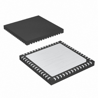
MAX8655ETN+ Maxim Integrated Products, MAX8655ETN+ Datasheet - Page 15

MAX8655ETN+
Manufacturer Part Number
MAX8655ETN+
Description
IC STEP-DN REG 25A 56-TQFN-EP
Manufacturer
Maxim Integrated Products
Type
Step-Down (Buck)r
Datasheets
1.MAX8655ETN.pdf
(24 pages)
2.MAX8655ETN.pdf
(23 pages)
3.MAX8655ETN.pdf
(24 pages)
4.MAX8655ETN.pdf
(24 pages)
Specifications of MAX8655ETN+
Internal Switch(s)
Yes
Synchronous Rectifier
No
Number Of Outputs
1
Voltage - Output
0.7 ~ 5.5 V
Current - Output
25A
Frequency - Switching
200kHz ~ 1MHz
Voltage - Input
4.5 ~ 25 V
Operating Temperature
-40°C ~ 85°C
Mounting Type
Surface Mount
Package / Case
56-TQFN Exposed Pad
Lead Free Status / RoHS Status
Lead free / RoHS Compliant
Power - Output
-
Lead Free Status / Rohs Status
Lead free / RoHS Compliant
To set the overvoltage threshold voltage for the
MAX8655, connect OVP to the center of an external
resistor-divider connected between the output and GND
(R4 and R6 of Figure 3). Select R6 between 5kΩ and
24kΩ, then calculate R4 with the following equation:
where V
There are several parameters that must be examined
when determining which inductor is to be used. Input
voltage, output voltage, load current, switching fre-
quency, and LIR. LIR is the ratio of the inductor current
ripple to the maximum DC load current. A higher LIR
value allows for a smaller inductor, but results in higher
losses and higher output ripple. A good compromise
between size and efficiency is an LIR of 0.3. Once all
the parameters are chosen, the inductor value is deter-
mined as follows:
where f
dard-value inductor close to the calculated value. The
exact inductor value is not critical and can be adjusted
to make trade-offs among size, cost, and efficiency.
Lower inductor values minimize size and cost, but they
also increase the output ripple and reduce the efficien-
cy due to higher peak currents. On the other hand,
higher inductor values increase efficiency, but eventu-
ally resistive losses due to extra turns of wire exceed
the benefit gained from lower AC current levels. This is
especially true if the inductance is increased without
also increasing the physical size of the inductor. Find a
low-loss inductor having the lowest possible DC resis-
tance that fits the allotted dimensions. The chosen
inductor’s saturation current rating must exceed the
peak inductor current determined as:
Setting the Output Overvoltage Protection
S
OVP
I
PEAK
is the switching frequency. Choose a stan-
= 1.15 x V
L
=
=
V
R
I
LOAD MAX
IN
4
______________________________________________________________________________________
V
=
×
OUT
Internal MOSFET, Step-Down Regulator
R
f
S
(
6
FB
×
×
×
.
I
LOAD MAX
⎛
⎜
⎝
(
)
V
V
V
+
OUT
IN
OVP
LIR
(
−
2
Highly Integrated, 25A, Wide-Input,
Inductor Selection
V
−
OUT
×
1
)
I
⎞
⎟
⎠
LOAD MAX
×
)
LIR
(
)
To set the switching frequency, connect a resistor from
FSYNC to GND. Calculate the resistor value in kΩ from
the following equation:
where f
For most applications where the duty cycle is less than
40%, connect SCOMP to GND to set the internal slope
compensation to the default of 125mV/T, where T is the
oscillator period (T = 1 / f
For a slope compensation of 250mV/T, connect
SCOMP to AVL.
For applications with a duty cycle greater than 40%, set
the SCOMP voltage with a resistor voltage-divider from
AVL to GND (R11 and R12 in Figure 6). First, use the
following equation to find the SCOMP voltage:
where R
is the minimum operating input voltage, and f
switching frequency.
Next, select a value for R11, typically 10kΩ, and solve
for R12 as follows:
This sets the internal slope-compensation voltage rate
to V
Figure 6. Resistor-Divider for Setting the Slope Compensation
SCOMP
V
S
SCOMP
L
is the desired switching frequency in kHz.
is the DC resistance of the inductor, V
/ (10 x T).
Setting the Switching Frequency
Setting the Slope Compensation
R
R
12
=
FSYNC
120
MAX8655
=
f
S
(
5
×
×
V V
=
L
R
−
SCOMP
30600
S
L
).
V
AVL
×
SCOMP
f
SCOMP
S
(
V
O
−
−
9 914
)
0 182
.
×
.
R12
R11
R
11
×
V
IN MIN
_
S
IN_MIN
is the
)
15


