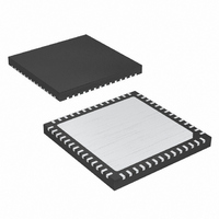
MAX8655ETN+ Maxim Integrated Products, MAX8655ETN+ Datasheet - Page 19

MAX8655ETN+
Manufacturer Part Number
MAX8655ETN+
Description
IC STEP-DN REG 25A 56-TQFN-EP
Manufacturer
Maxim Integrated Products
Type
Step-Down (Buck)r
Datasheets
1.MAX8655ETN.pdf
(24 pages)
2.MAX8655ETN.pdf
(23 pages)
3.MAX8655ETN.pdf
(24 pages)
4.MAX8655ETN.pdf
(24 pages)
Specifications of MAX8655ETN+
Internal Switch(s)
Yes
Synchronous Rectifier
No
Number Of Outputs
1
Voltage - Output
0.7 ~ 5.5 V
Current - Output
25A
Frequency - Switching
200kHz ~ 1MHz
Voltage - Input
4.5 ~ 25 V
Operating Temperature
-40°C ~ 85°C
Mounting Type
Surface Mount
Package / Case
56-TQFN Exposed Pad
Lead Free Status / RoHS Status
Lead free / RoHS Compliant
Power - Output
-
Lead Free Status / Rohs Status
Lead free / RoHS Compliant
The crossover frequency, f
than the power-modulator pole f
be less than or equal to 1/5 the switching frequency.
Select a value for f
At the crossover frequency, the total loop gain must
equal 1, and is expressed as:
For the case where f
Then R
where g
The error-amplifier compensation zero formed by R
and C
Calculate the value of C
If f
from COMP to GND. The value of C
As the load current decreases, the modulator pole
also decreases; however, the modulator gain increases
accordingly and the crossover frequency remains
the same.
For the case where f
The power modulator gain at f
zMOD
C
C
mEA
is less than 5 x f
should be set at the modulator pole f
can be calculated as:
= 110µS.
G
G
R
G
MOD fc
MOD fc
C
EA fc
C
C
=
G
( )
C
F
______________________________________________________________________________________
C
f
pMOD
( )
( )
g
EA fc
=
=
in the range:
mEA
Internal MOSFET, Step-Down Regulator
×
zMOD
zMOD
( )
2π
2π
=
=
G
C
G
G
MOD fc
×
×
=
×
<<
C
MOD dc
MOD dc
as follows:
R
f
V
, add a second capacitor C
g
p MOD
V
is greater than f
is less than f
FB
C
mEA
C
f
C
OUT
( )
1
1
, should be much higher
×
C
(
(
≤
×
Highly Integrated, 25A, Wide-Input,
f
zMOD
is:
G
f
×
5
S
×
PMOD
)
)
×
MOD fc
R
×
V
×
R
V
F
OUT
C
C
f
f
f
FB
pMOD
pMOD
zMOD
is:
f
( )
. Also, f
C
= 1
C
:
C
:
C
should
PMOD
C
F
.
The error-amplifier gain at f
Figure 11 is the simplified gain plot for the f
case.
R
where g
C
C
The current-mode control model on which the above
design procedure is based requires an additional high-
frequency term, G
pling the peak inductor current. The term G
produces additional phase lag at crossover and should
be modeled to estimate the phase margin obtainable
by the selected compensation components. As a final
step, it is useful to plot the dB gain and phase of the
following loop-gain transfer function and check the
Figure 11. Simplified Gain Plot for the f zMOD < f C Case
C
C
F
POWER
MODULATOR
is calculated from:
is calculated as:
is calculated from:
GAIN
(dB)
0dB
mEA
R
C
=
= 110µS.
FB
DIVIDER
G
V
V
OUT
EA fc
FB
C
C
( )
F
C
S
=
(s), to account for the effect of sam-
×
=
fp
MOD
=
2π
g
2π
g
mEA
mEA
CLOSED LOOP
×
×
R
f
p MOD
C
C
×
1
×
is:
1
G
×
fz
MOD
R
MOD fc
f
zMOD
C
×
f
C
×
R
( )
f
fc
C
zMOD
f
C
×
ERROR
AMPLIFIER
f
zMOD
zMOD
FREQUENCY
< f
S
(s)
19
C


