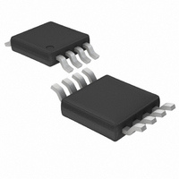
LT1949-1EMS8#TR Linear Technology, LT1949-1EMS8#TR Datasheet - Page 5

LT1949-1EMS8#TR
Manufacturer Part Number
LT1949-1EMS8#TR
Description
IC CONV DC/DC PWM STEP UP 8MSOP
Manufacturer
Linear Technology
Type
Step-Up (Boost)r
Datasheet
1.LT1949-1EMS8TR.pdf
(8 pages)
Specifications of LT1949-1EMS8#TR
Internal Switch(s)
Yes
Synchronous Rectifier
No
Number Of Outputs
1
Voltage - Output
Adj to 28V
Current - Output
1A
Frequency - Switching
1.1MHz
Voltage - Input
1.7 ~ 12 V
Operating Temperature
-40°C ~ 85°C
Mounting Type
Surface Mount
Package / Case
8-MSOP, Micro8™, 8-uMAX, 8-uSOP,
Lead Free Status / RoHS Status
Contains lead / RoHS non-compliant
Power - Output
-
Available stocks
Company
Part Number
Manufacturer
Quantity
Price
BLOCK DIAGRA
OPERATIO
The LT1949-1 is a current mode, fixed frequency step-up
DC/DC converter with an internal 1A NPN power transis-
tor. Operation can best be understood by referring to the
Block Diagram.
At the beginning of each oscillator cycle, the flip-flop is set
and the switch is turned on. Current in the switch ramps
up until the voltage at A2’s positive input reaches the V
pin voltage, causing A2’s output to change state and the
switch to be turned off. The signal at A2’s positive input is
a summation of a signal representing switch current and
a ramp generator (introduced to avoid subharmonic oscil-
lations at duty factors greater than 50%). If the load
increases, V
amplifier will drive V
in the switch to increase. In this way, the error amplifier
drives the V
load. Frequency compensation is provided by an external
series RC network connected between the V
ground.
C
OUT
pin to the voltage necessary to satisfy the
V
OUT
REFERENCE
(and FB) will drop slightly and the error
R1
(EXTERNAL)
R2
(EXTERNAL)
U
1.24V
FB
C
to a higher voltage, causing current
W
FB
2
+
–
OSCILLATOR
GENERATOR
1.1MHz
RAMP
g
AMPLIFIER
m
ERROR
Figure 3. LT1949-1 Block Diagram
C
pin and
+
+
BIAS
C
V
+
–
–
+
1
C
Layout Hints
The LT1949-1 switches current at high speed, mandating
careful attention to layout for proper performance. You
will not get advertised performance with careless layouts.
Figure 4 shows recommended component placement for
a boost (step-up) converter. Follow this closely in your PC
layout. Note the direct path of the switching loops. Input
capacitor C1 must be placed close (< 5mm) to the IC
package. As little as 10mm of wire or PC trace from C
V
oscillation.
The ground terminal of output capacitor C2 should tie
close to Pin 4 of the LT1949-1. Doing this reduces dI/dt in
the ground copper which keeps high frequency spikes to
a minimum. The DC/DC converter ground should tie to the
PC board ground plane at one place only, to avoid intro-
ducing dI/dt in the ground plane.
A2
COMPARATOR
A1
COMPARATOR
IN
will cause problems such as inability to regulate or
ENABLE
R
200mV
FF
S
LBI
7
Q
–
+
A = 2
SHUTDOWN
A4
+
–
DRIVER
SHDN
GND
LBO
SW
8
3
5
4
Q3
0.06
1949-1 BD
LT1949-1
IN
5
to


