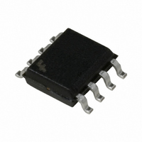
FAN6520AMX Fairchild Semiconductor, FAN6520AMX Datasheet - Page 9

FAN6520AMX
Manufacturer Part Number
FAN6520AMX
Description
IC CTRLR PWM SYNC BUCK SGL 8SOIC
Manufacturer
Fairchild Semiconductor
Type
Step-Down (Buck)r
Datasheet
1.FAN6520AMX.pdf
(15 pages)
Specifications of FAN6520AMX
Internal Switch(s)
No
Synchronous Rectifier
Yes
Number Of Outputs
1
Voltage - Output
0.8 ~ 5.5 V
Frequency - Switching
300kHz
Voltage - Input
4.5 ~ 5.5 V
Operating Temperature
0°C ~ 70°C
Mounting Type
Surface Mount
Package / Case
8-SOIC (3.9mm Width)
Power - Output
715mW
Topology
Boost, Buck
Output Voltage
0.8 V to 5.5 V
Switching Frequency
340 KHz
Duty Cycle (max)
100 %
Operating Supply Voltage
5 V
Maximum Operating Temperature
+ 70 C
Minimum Operating Temperature
0 C
Mounting Style
SMD/SMT
Synchronous Pin
No
Lead Free Status / RoHS Status
Lead free / RoHS Compliant
Current - Output
-
Lead Free Status / Rohs Status
Lead free / RoHS Compliant
Other names
FAN6520AMXTR
FAN6520AMX_NL
FAN6520AMX_NLTR
FAN6520AMX_NLTR
FAN6520AMX_NL
FAN6520AMX_NLTR
FAN6520AMX_NLTR
Available stocks
Company
Part Number
Manufacturer
Quantity
Price
Part Number:
FAN6520AMX_
Manufacturer:
FAIRCHILD/ن»™ç«¥
Quantity:
20 000
©2005 Fairchild Semiconductor Corporation
FAN6520A Rev. 1.0.5
An output capacitor is required to filter the output and
supply the load transient current. The filtering require-
ments are a function of the switching frequency and the
ripple current. The load transient requirements are a
function of the slew rate (di/dt) and the magnitude of the
transient load current. These requirements are generally
met with a mix of capacitors and careful layout.
Component Selection
Output Capacitors (C
Modern components and loads are capable of producing
transient load rates above 1A/ns. High-frequency capac-
itors initially supply the transient and slow the current
load rate seen by the bulk capacitors. Effective Series
Resistance (ESR) and voltage rating are typically the
prime considerations for the bulk filter capacitors, rather
than actual capacitance requirements. High-frequency
decoupling capacitors should be placed as close to the
power pins of the load as physically possible. Be careful
not to add inductance in the circuit board wiring that
could cancel the performance of these low-inductance
components. Consult with the load manufacturer on spe-
cific decoupling requirements. Use only specialized low-
ESR capacitors intended for switching-regulator applica-
tions for the bulk capacitors. The bulk capacitor’s ESR
determines the output ripple voltage and the initial volt-
age drop after a high slew-rate transient. An aluminum
electrolytic capacitor’s ESR value is related to the case
size with lower ESR available in larger case sizes; how-
ever, the Equivalent Series Inductance (ESL) of these
capacitors increases with case size and can reduce the
usefulness of the capacitor to high slew-rate transient
loading. Since ESL is not a specified parameter, work
with the capacitor supplier and measure the capacitor’s
impedance with frequency to select a suitable compo-
nent. Generally, multiple small-case electrolytic capaci-
tors perform better than a single large-case capacitor.
Figure 8. Asymptotic Bode Plot of Converter Gain
100
-20
-40
-60
80
60
40
20
0
10
(R
20LOG
2
MODULATOR
/R
1
)
GAIN
100
1K
F
Z1
F
FREQUENCY (Hz)
LC
F
OUT
Z2
10K
)
F
F
P1
ESR
(V
IN
100K
20LOG
/DV
F
P2
OSC
OPEN LOOP
ERROR AMP GAIN
)
1M
COMPENSATION
CLOSED LOOP
10M
GAIN
GAIN
Output Inductor (L
The output inductor is selected to meet the output volt-
age ripple requirements and minimize the converter’s
response time to the load transient. The inductor value
determines the converter’s ripple current and the ripple
voltage is a function of the ripple current. The ripple volt-
age (ΔV) and current (ΔI) are approximated by the fol-
lowing equations:
Increasing the inductance value reduces the ripple cur-
rent and voltage, but also reduces the converter’s ability
to quickly respond to a load transient. One of the param-
eters limiting the converter’s response to a load transient
is the time required to change the inductor
Given a sufficiently fast control-loop design, the
FAN6520A provides either 0% or 100% duty cycle in
response to a load transient. The response time is the
time required to slew the inductor current from an initial
current value to the transient current level. During this
interval, the difference between the inductor current and
the transient current level must be supplied by the output
capacitor. Minimizing the response time can minimize
the output capacitance required.
Depending on whether there is a load application or a
load removal, the response time to a load transient
(I
approximate response time interval for application and
removal of a transient load:
where T
positive I
removal (negative I
can be either at application or removal of load. Check
both of these equations at the minimum and maximum
output levels for the worst-case response time.
Input Capacitor Selection
Use a mix of input bypass capacitors to control the volt-
age overshoot across the MOSFETs. Use small ceramic
capacitors for high-frequency decoupling and bulk
capacitors to supply the current needed each time Q1
turns on. Place the small ceramic capacitors physically
close to the MOSFETs and between the drain of Q1 and
the source of Q2. The important parameters for the bulk
input capacitor are the voltage rating and the RMS cur-
rent rating. For reliable operation, select the bulk capaci-
tor with voltage and current ratings above the maximum
input voltage and the largest RMS current required by
the circuit. The capacitor voltage rating should be at least
T
T
ΔI
STEP
RISE
FALL
9
=
) is different. The following equations give the
⎛
⎜
⎝
V
----------------------------- -
=
=
RISE
IN
F
STEP
----------------------------- -
V
L
------------------------
SW
L
–
IN
×
V
×
V
is the response time to the application of a
OUT
I
×
–
STEP
I
OUT
and T
STEP
L
V
OUT
⎞
⎟
⎠
STEP
×
FALL
OUT
V
--------------
V
OUT
). The worst-case response time
IN
is the response time to a load
)
ΔV ESR
≈
×
www.fairchildsemi.com
ΔI
current.
(10)
(11)
(9)


