NJU7262M30 NJR, NJU7262M30 Datasheet

IC SW-REG STEP-UP 3V 8-DMP

NJU7262M30

Manufacturer Part Number
NJU7262M30
Description
IC SW-REG STEP-UP 3V 8-DMP
Manufacturer
NJR
Type
Step-Up (Boost)r
Datasheet

Specifications of NJU7262M30

Internal Switch(s)
Yes
Synchronous Rectifier
No
Number Of Outputs
1
Voltage - Output
3V
Current - Output
250mA
Frequency - Switching
30kHz
Voltage - Input
1 ~ 10 V
Operating Temperature
-25°C ~ 75°C
Mounting Type
Surface Mount
Package / Case
8-DMP
Power - Output
300mW
Mounting Style
SMD/SMT
Lead Free Status / RoHS Status
Contains lead / RoHS non-compliant
■ GENERAL DESCRIPTION
which contains accurate voltage reference, error amplifier, CR
oscillator, control circuit, switching transistor, diode and resistor.
from external, and the stand-by function is effective for low power
consumption.
line-up of different output voltages version are available.
items because of its small packaged outline, low operating voltage
and current.
■ FEATURES
■ LINE-UP
■ TERMINAL DESCRIPTION
Ver.2009-03-25
Output Voltage (V)
The NJU7262 series is a C-MOS step-up switching regulator
The operating clock is prepared on-chip or is available to input
The regulation voltage is fixed by internal circuits and the following
• Low Operating Voltage
• Low Operating Current
• Low Stand-by Current
• High Precision Output Voltage (±3% max.)
• Wide Operating Voltage Range
• External/Internal Clock Select Function
• Stand-by Function
• CR Oscillator On-chip
• Diode On-chip
• Package Outline
• C-MOS Technology
This series is suitable for portable equipment's or battery operated
No.
1
2
3
4
5
6
7
8
3.0
5.0
Term. Name
CONT
GND
V
STB
CLK
SW
NC
V
OUT
IN
NJU7262M30
NJU7262M50
DMP-8
C-MOS STEP-UP SWITCHING REGULATOR
POWER
POWER
(1.0V min.)
(5.0µA typ. / V
(0.2µA max. / V
DMP-8/SSOP-8/VSP-8
I/O
O
-
I
I
I
I
NJU7262V30
NJU7262V50
Package
SSOP-8
External Inductor Connect Terminal
Power Source (GND)
Non Connect
Strobe Terminal : "H" ···Normal Operation (step-up)
Power Source (+)
External / Internal
External Clock Input Terminal
Step-up Output Terminal
Clock Select Terminal
OUT
OUT
= 3.0V)
= 3.0V)
NJU7262R30
NJU7262R50
(When "L" level is input, Internal oscillation is stopped)
VSP-8
" L " ···Stand-By Operation
"H" or OPEN···Internal Oscillation
■ PACKAGE OUTLINE
■ PIN CONFIGURATION
■ EQUIVALENT CIRCUIT
"L"
FUNCTION
NJU7262VXX
NJU7262MXX
···External Clock Input
NJU7262RXX
PRELIMINARY
- 1 -

Related parts for NJU7262M30

NJU7262M30 Summary of contents

Page 1

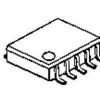
... Wide Operating Voltage Range • External/Internal Clock Select Function • Stand-by Function • CR Oscillator On-chip • Diode On-chip • Package Outline • C-MOS Technology ■ LINE-UP Output Voltage (V) DMP-8 3.0 NJU7262M30 5.0 NJU7262M50 ■ TERMINAL DESCRIPTION No. Term. Name 1 CONT 2 GND 3 ...

Page 2

ABSOLUTE MAXIMUM RATINGS PARAMETER Input Voltage CONT Input Voltage STB, SW, CLK Input Voltage Output Voltage Power Dissipation Operating Temperature Range Storage Temperature Range Note) Decoupling capacitor should be connected between V converter. ■ ELECTRICAL CHARACTERISTICS +3V Version PARAMETER ...

Page 3

Version PARAMETER SYMBOL Input Voltage V Start Voltage V START Oscillator Freq. f OSC Output Voltage V OUT Input Stability ∆V OUT1 Load Stability ∆V OUT2 Operating Current I SS Stand-by Current I Q Switching Current ...

Page 4

MEASUREMENT CIRCUIT (1) (2) ( External Diode Type : "D1NS4" provided by SHINDENGEN ( 0.55V) V OUT OUT ...

Page 5

Ver.2009-03- ...

Page 6

APPLICATION CIRCUIT - 6 - [CAUTION] The specifications on this databook are only given for information , without any guarantee as regards either mistakes or omissions. The application circuits in this databook are described only to show ...

Related keywords