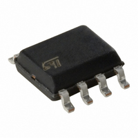
ST662ABD STMicroelectronics, ST662ABD Datasheet - Page 11

ST662ABD
Manufacturer Part Number
ST662ABD
Description
IC CONV DC/DC 5V-12V .03A 8SOIC
Manufacturer
STMicroelectronics
Type
Switched Capacitor (Charge Pump)r
Datasheet
1.ST662ACD-TR.pdf
(20 pages)
Specifications of ST662ABD
Internal Switch(s)
Yes
Synchronous Rectifier
No
Number Of Outputs
1
Voltage - Output
11.4 ~ 12.6 V
Current - Output
30mA
Frequency - Switching
400kHz
Voltage - Input
4.5 ~ 5.5 V
Operating Temperature
-40°C ~ 85°C
Mounting Type
Surface Mount
Package / Case
8-SOIC (3.9mm Width)
Power - Output
500mW
Output Voltage
12.6 V
Mounting Style
SMD/SMT
Lead Free Status / RoHS Status
Lead free / RoHS Compliant
Other names
497-2104-5
Available stocks
Company
Part Number
Manufacturer
Quantity
Price
Company:
Part Number:
ST662ABD-TR
Manufacturer:
TRIQUINT
Quantity:
920
Company:
Part Number:
ST662ABD-TR
Manufacturer:
STMicroelectronics
Quantity:
45 661
Part Number:
ST662ABD-TR
Manufacturer:
ST
Quantity:
20 000
Company:
Part Number:
ST662ABD-TRY
Manufacturer:
STMicroelectronics
Quantity:
29 931
ST662AB, ST662AC
7
Figure 15. KIT layout
Application circuit
Based on fast charge/discharge of capacitors, this circuit involves high di/dt values limited
only by R
inductive paths and place capacitors as close as possible to the device.
A good layout design is strongly recommended for noise reason. For best performance, use
very short connections to the capacitors and the values shown in
C3 and C4 must have low ESR in order to minimize the output ripple. Their values can be
reduced to 2 µF and 1 µF, respectively, when using ceramic capacitors, but must be of 10 µF
or larger if aluminium electrolytic are chosen.
C5 must be placed as close to the device as possible and could be omitted if very low output
noise performance are not required.
Figure 15
ON
and
of switches. This implies a critical layout design due to the need to minimize
Figure 16
show, respectively, our EVALUATION kit layout and the relatively.
Doc ID 5068 Rev 8
Table
7.
Application circuit
11/20


