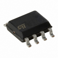
ST755CD STMicroelectronics, ST755CD Datasheet

ST755CD
Specifications of ST755CD
Available stocks
Related parts for ST755CD
ST755CD Summary of contents
Page 1
... 25° logic controlled shut down pin that interfaces directly with microprocessor reduces supply current to only 10mA. Input to Output differential voltage is limited to V supply current is 1.2mA = -5V O Package ST755CD-TR Rev. 5 ST755C SO-8 = -5V). O +|V |<12.7V. No load I O Packaging SO-8 (tape & reel) www.st.com ...
Page 2
Contents 1 Diagram . . . . . . . . . . . . . . . . . . . . . . . . . . . . . . . . . . . . . ...
Page 3
Diagram Figure 1. Schematic diagram 3/16 ...
Page 4
Pin configuration Figure 2. Pin connections (top view) Table 2. Pin description Pin N° Symbol 1 SHDN SHUT-DOWN control ( Reference output voltage: (1.25V) REF 3 SS Soft start 4 CC Compensation input 5 V Negative output ...
Page 5
Maximum ratings Table 3. Absolute maximum ratings Symbol V DC input voltage to GND CC V Shutdown voltage, SS Voltage, CC Voltage SHDN V Switch voltage ( Feedback voltage ( Peak switch current ...
Page 6
Electrical characteristics Table 5. Electrical characteristics (Refer to the test circuits 0mA LOAD 25°C) A Symbol Parameter V Input voltage I V Output voltage O I Output current O Supply ...
Page 7
Application information The ST755 developed for voltage conversion from an input voltage ranging from +2.4V to 11V to a regulated adjustable negative output limited by |V circuit adopts a current-mode PWM control scheme to achieve good ...
Page 8
Application circuit To achieve the best performances from switching power supply topology, particular care to layout drawing is needed, in order to minimize EMI and obtain low noise, jitter free operation moreover, it ensures the full device functionality. Layout ...
Page 9
Figure 4. Printed demoboard Note: Drawings not in scale Table 6. Component values Capacitor Value C1 C2 100 Unit Resistor 47 µF R1 µ µ µ ...
Page 10
Typical performance characteristics (Unless otherwise specified T Figure 5. Load current vs supply voltage Figure 7. Load current vs supply voltage Figure 9. Efficiency vs load current 10/16 = 25°C) J Figure 6. Peak inductor current vs load curr. ...
Page 11
Figure 11. Switch current limit vs soft start voltage Figure 13. Soft start delay time Figure 12. Reference voltage vs temperature 11/16 ...
Page 12
Package mechanical data In order to meet environmental requirements, ST offers these devices in ECOPACK packages. These packages have a Lead-free second level interconnect. The category of second Level Interconnect is marked on the package and on the inner ...
Page 13
SO-8 MECHANICAL DATA mm. DIM. MIN. TYP A 1.35 A1 0.10 A2 1.10 B 0.33 C 0.19 D 4.80 E 3.80 e 1.27 H 5.80 h 0.25 L 0.40 k ddd inch MAX. MIN. TYP. 1.75 0.053 0.25 0.04 1.65 ...
Page 14
Tape & Reel SO-8 MECHANICAL DATA DIM. MIN 12 8.1 Bo 5.5 Ko 2.1 Po 3.9 P 7.9 14/16 mm. TYP MAX. MIN. 330 13.2 0.504 0.795 2.362 22.4 8.5 0.319 5.9 ...
Page 15
Revision history Table 7. Revision history Date Revision 06-Jul-2007 5 Changes Device summary updated and the document has been reformatted. 15/16 ...
Page 16
... Information in this document is provided solely in connection with ST products. STMicroelectronics NV and its subsidiaries (“ST”) reserve the right to make changes, corrections, modifications or improvements, to this document, and the products and services described herein at any time, without notice. All ST products are sold pursuant to ST’s terms and conditions of sale. ...


