MC33166T ON Semiconductor, MC33166T Datasheet - Page 15
MC33166T
Manufacturer Part Number
MC33166T
Description
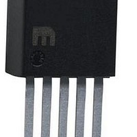
IC REG SWITCH INVERT 3A TO220-5
Manufacturer
ON Semiconductor
Type
Step-Down (Buck), Step-Up (Boost), Invertingr
Datasheet
1.MC34166TG.pdf
(18 pages)
Specifications of MC33166T
Internal Switch(s)
Yes
Synchronous Rectifier
No
Number Of Outputs
1
Voltage - Output
1.25 ~ 40 V
Current - Output
3A
Frequency - Switching
72kHz
Voltage - Input
7.5 ~ 40 V
Operating Temperature
-40°C ~ 85°C
Mounting Type
Through Hole
Package / Case
TO-220-5 (Straight Leads)
Mounting Style
Through Hole
Lead Free Status / RoHS Status
Contains lead / RoHS non-compliant
Power - Output
-
Lead Free Status / Rohs Status
Lead free / RoHS Compliant
Other names
MC33166TOS
Available stocks
Company
Part Number
Manufacturer
Quantity
Price
Company:

Part Number:
MC33166T
Manufacturer:
MOT
Quantity:
5 510
Part Number:
MC33166T
Manufacturer:
ON/安森美
Quantity:
20 000
Company:
Part Number:
MC33166TG
Manufacturer:
SAKEN
Quantity:
20 000
Part Number:
MC33166TG
Manufacturer:
ON/安森美
Quantity:
20 000
Company:
Part Number:
MC33166TV
Manufacturer:
ON
Quantity:
20 000
Company:
Part Number:
MC33166TVG
Manufacturer:
ON Semiconductor
Quantity:
350


1. V
2. V
3. Duty cycle is calculated at the minimum operating input voltage and must not exceed the guaranteed minimum DC
The following converter characteristics must be chosen:
V
ripple(pp)
sat
F
Calculation
(Notes 1, 2)
Duty Cycle
− Output rectifier forward voltage drop. Typical value for 1N5822 Schottky barrier rectifier is 0.5 V.
V
V
I
I
DI
(Note 3)
pk(switch)
− Switch Output source saturation voltage, refer to Figure 8.
out
out
ripple(pp)
I
L
L avg
V
t on
t off
t
L
on
out
−
−
−
−
Desired output voltage.
Desired output current.
Desired peak−to−peak inductor ripple current. For maximum output current especially when the duty cycle is greater than
0.5, it is suggested that DI
I
Desired peak−to−peak output ripple voltage. For best performance, the ripple voltage should be kept to less than 2% of V
Capacitor C
pk(switch)
inductance value, let DI
from reaching the guaranteed minimum current limit threshold of 3.3 A. If the design goal is to use a minimum
O
DI L
should be a low equivalent series resistance (ESR) electrolytic designed for switching regulator applications.
V in * V sat * V out
V in * V sat * V out
I L avg )
f osc
V ref
8f osc C o
Step−Down
V out ) V F
t
DI L
1
L
on
t on
t off
R 2
R 1
t on
t off
I
= 2 (I
out
L
f
osc
be chosen to be less than 10% of the average inductor current I
) 1
) 1
2 ) (ESR) 2
DI L
L avg
2
). This will proportionally reduce the converter’s output current capability.
t on
Table 1. Design Equations
MC34166, MC33166
http://onsemi.com
t on
t off
V in * V satQ1 * V satQ2
V in * V satQ1 * V satQ2
) 1
15
V out ) V F1 ) V F2
Step−Up/Down
f osc
I L avg )
V ref
I out
t
DI L
f osc C o
on
t on
t off
t on
t off
R 2
R 1
t on
t off
f
1
osc
) 1
) 1
) 1
DI L
2
2 ) (ESR) 2
t on
t on
t off
L avg
) 1
Voltage−Inverting
. This will help prevent
f osc
I L avg )
V in * V sat
V ref
I out
|V out | ) V F
V in * V sat
(max)
t
DI L
f osc C o
on
t on
t off
t on
t off
R 2
R 1
t on
t off
f
1
specification of 0.92.
osc
) 1
) 1
) 1
DI L
2
t on
2 ) (ESR) 2
out
.
Related parts for MC33166T
Image
Part Number
Description
Manufacturer
Datasheet
Request
R

Part Number:
Description:
ON Semiconductor [VOLTAGE REGULATOR]
Manufacturer:
ON Semiconductor
Datasheet:
Part Number:
Description:
357-036-542-201 CARDEDGE 36POS DL .156 BLK LOPRO
Manufacturer:
ON Semiconductor
Datasheet:
Part Number:
Description:
357-036-542-201 CARDEDGE 36POS DL .156 BLK LOPRO
Manufacturer:
ON Semiconductor
Datasheet:
Part Number:
Description:
357-036-542-201 CARDEDGE 36POS DL .156 BLK LOPRO
Manufacturer:
ON Semiconductor
Datasheet:
Part Number:
Description:
357-036-542-201 CARDEDGE 36POS DL .156 BLK LOPRO
Manufacturer:
ON Semiconductor
Datasheet:
Part Number:
Description:
357-036-542-201 CARDEDGE 36POS DL .156 BLK LOPRO
Manufacturer:
ON Semiconductor
Datasheet:
Part Number:
Description:
357-036-542-201 CARDEDGE 36POS DL .156 BLK LOPRO
Manufacturer:
ON Semiconductor
Datasheet:
Part Number:
Description:
357-036-542-201 CARDEDGE 36POS DL .156 BLK LOPRO
Manufacturer:
ON Semiconductor
Datasheet:
Part Number:
Description:
357-036-542-201 CARDEDGE 36POS DL .156 BLK LOPRO
Manufacturer:
ON Semiconductor
Datasheet:
Part Number:
Description:
357-036-542-201 CARDEDGE 36POS DL .156 BLK LOPRO
Manufacturer:
ON Semiconductor
Datasheet:
Part Number:
Description:
357-036-542-201 CARDEDGE 36POS DL .156 BLK LOPRO
Manufacturer:
ON Semiconductor
Datasheet:
Part Number:
Description:
Manufacturer:
ON Semiconductor
Datasheet:
Part Number:
Description:
Manufacturer:
ON Semiconductor
Datasheet:
Part Number:
Description:
Manufacturer:
ON Semiconductor
Datasheet: