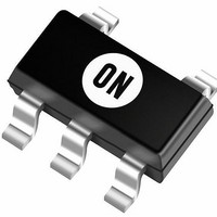
MAX829EUK ON Semiconductor, MAX829EUK Datasheet - Page 6

MAX829EUK
Manufacturer Part Number
MAX829EUK
Description
IC INVERTER CHARGE PUMP SOT23-5
Manufacturer
ON Semiconductor
Type
Switched Capacitor (Charge Pump), Doubler, Invertingr
Datasheet
1.MAX829EUK.pdf
(17 pages)
Specifications of MAX829EUK
Internal Switch(s)
Yes
Synchronous Rectifier
No
Number Of Outputs
1
Voltage - Output
-1.15 ~ -5.5 V, 2.3 ~ 11 V
Current - Output
50mA
Frequency - Switching
19kHz ~ 54kHz
Voltage - Input
1.15 ~ 5.5 V
Operating Temperature
-40°C ~ 85°C
Mounting Type
Surface Mount
Package / Case
TSOT-23-5, TSOT-5, TSOP-5
Power - Output
313mW
Function
Inverting
Output Voltage
- 5.5 V to - 1.15 V
Output Current
100 mA
Maximum Operating Temperature
+ 150 C
Mounting Style
SMD/SMT
Lead Free Status / RoHS Status
Contains lead / RoHS non-compliant
Other names
MAX829EUKOS
Available stocks
Company
Part Number
Manufacturer
Quantity
Price
Company:
Part Number:
MAX829EUK
Manufacturer:
MAXIM
Quantity:
5 321
Company:
Part Number:
MAX829EUK
Manufacturer:
MAX
Quantity:
356
Company:
Part Number:
MAX829EUK+T
Manufacturer:
Intersil
Quantity:
230
Company:
Part Number:
MAX829EUK+T
Manufacturer:
MAXIN
Quantity:
10
Part Number:
MAX829EUK+T
Manufacturer:
MAXIM/美信
Quantity:
20 000
Part Number:
MAX829EUKG
Manufacturer:
ON/安森美
Quantity:
20 000
DETAILED OPERATING DESCRIPTION
voltage applied to the V
two−phase operation (Figure 21). During the first phase,
switches S
this time, C
is supplied from C
closed, and S
across C
APPLICATIONS INFORMATION
Output Voltage Considerations
not provide regulation. The output voltage will drop in a
linear manner with respect to load current. The value of this
equivalent output resistance is approximately 26 W nominal
at 25°C and V
loads, and drops according to the equation below:
V
The MAX828/829 charge pump converters inverts the
The MAX828/829 performs voltage conversion but does
Figure 21. Ideal Switched Capacitor Charge Pump
in
V
From Osc
in
2
Figure 20. Test Setup/Voltage Inverter
, restoring charge to C
+
2
C
1
and S
MAX828: C
MAX829: C
3
charges to the voltage on V
in
S1
S3
1
V out + * (V in * V DROP )
1
2
3
= 5.0 V. V
and S
V DROP + I out
4
2
are open and S
. During the second phase, S
C
OSC
1
3
1
1
are open. This action connects C
= C
= C
out
in
2
2
S2
S4
is approximately −5.0 V at light
pin. Conversion consists of a
= C
= C
6
4
3
3
2
1
.
= 3.3 mF
= 10 mF
and S
R out
C
3
in
2
are closed. During
+
C
and load current
1
+
C
−V
2
2
out
and S
MAX828, MAX829
−V
http://onsemi.com
out
R
4
L
are
1
6
Charge Pump Efficiency
affected by four factors:
These losses are given by Equation 1.
resistance of an ideal switched capacitor circuit (Figures 22
and 23).
Equation 2. The output voltage ripple is given by Equation 3.
P LOSS + [ 0.5C 1 (V in
The overall power efficiency of the charge pump is
Most of the conversion losses are due to factors 2, 3 and 4.
The 1/(f
The losses due to charge transfer above are also shown in
1. Losses from power consumed by the internal
2. I
3. Charge pump capacitor losses due to Equivalent
4. Losses that occur during charge transfer from the
V
V
(f
in
oscillator, switch drive, etc. (which vary with input
voltage, temperature and oscillator frequency).
switches on−board the charge pump.
Series Resistance (ESR).
commutation capacitor to the output capacitor when
a voltage difference between the two capacitors
exists.
P
V
in
OSC
Figure 22. Ideal Switched Capacitor Model
2
LOSS(2,3,4)
Figure 23. Equivalent Output Resistance
R losses due to the on−resistance of the MOSFET
) 0.5C 2 (V RIPPLE
RIPPLE
1
R
OSC
EQUIV
)C 1
)(C
) 8R
1
+
R
) term in Equation 1 is the effective output
+
f
EQUIV
(f
f
+ I out
OSC
C
SWITCH
1
1
2
I out
C 1
* V out
)(C 2 )
2
2
* 2V out V RIPPLE )]
) 4ESR
) 2(I out )(ESR
R out ^ I out
2
)
C
C
C 1
2
2
) ESR
2
R
R
C 2
L
L
)
C 2
V
V
(eq. 3)
out
f OSC
out
(eq. 2)
(eq. 1)


