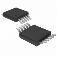
LT3750EMS#PBF Linear Technology, LT3750EMS#PBF Datasheet - Page 4

LT3750EMS#PBF
Manufacturer Part Number
LT3750EMS#PBF
Description
IC CTLR CAPACITOR CHARGE 10-MSOP
Manufacturer
Linear Technology
Type
Flyback, Forward Converterr
Datasheet
1.LT3750EMSPBF.pdf
(16 pages)
Specifications of LT3750EMS#PBF
Applications
Power Supply Controller
Mounting Type
Surface Mount
Package / Case
10-MSOP, Micro10™, 10-uMAX, 10-uSOP
Ic Function
Capacitor Charger Controller
Supply Voltage Range
3V To 24V
Operating Temperature Range
-40°C To +85°C
Digital Ic Case Style
MSOP
No. Of Pins
10
Msl
MSL 1 - Unlimited
Rohs Compliant
Yes
Lead Free Status / RoHS Status
Lead free / RoHS Compliant
Available stocks
Company
Part Number
Manufacturer
Quantity
Price
PI FU CTIO S
LT3750
V
primary coil of the transformer as well as internal circuitry
that performs boundary mode detection. Bypass at the pin
with a 1µF to 10µF capacitor. Bypass the primary winding
of the transformer with a large capacitor.
DONE (Pin 2): Open Collector Indication Pin. When target
output voltage is reached, an NPN transistor turns on.
Requires a pull-up resistor or current source. Any fault
conditions such as thermal shutdown or undervoltage
lockout will also turn on the NPN.
CHARGE (Pin 3): Charge Pin. Initiates a new charge cycle
when brought high or discontinues charging and puts part
into shutdown when low. To properly enable the device, a
step input with a minimum ramp rate of 1V/µs is required.
Drive to 1.1V or higher to enable the device; drive below
0.2V to disable the device.
V
ceramic capacitor. A 1µF to 10µF ceramic capacitor should
be sufficient for most applications.
GND (Pin 5): Ground Pin. Connect directly to local ground
plane.
4
TRANS
CC
U
(Pin 4): Input Supply Pin. Bypass locally with a
(Pin 1): Transformer Supply Pin. Powers the
U
U
SOURCE (Pin 6): Source Pin. Senses NMOS drain current.
Connect NMOS source terminal and current sense resistor
to this pin. The current limit is 78mV/R
GATE (Pin 7): Gate Pin. Connect NMOS gate terminal to
this pin. Internal gate driver will drive voltage to within
V
RDCM (Pin 8): Discontinuous Mode Sense Pin. Senses
when current in transformer has decayed to zero and ini-
tiates a new charge cycle if output voltage target has not
been reached. Place a resistor between this pin and the drain
of the NMOS. A good choice is a 43k, 5% resistor.
RV
a current proportional to output capacitor voltage. Con-
nect a resistor between this pin and the drain of the NMOS.
RBG (Pin 10): Output Voltage Sense Pin. Senses the
voltage across the RBG resistor, which is proportional to
the current flowing into the R
equals 1.24V, charging is disabled and DONE pin goes
low. Connect a resistor (2.5k or less is recommended)
from this pin to GND. A 2.49k, 1% resistor is a good
choice.
CC
OUT
– 2V during each switching cycle.
(Pin 9): Output Voltage VI Converter Pin. Develops
VOUT
pin. When voltage
SENSE
.
3750fa


