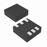
MAX4866LELT+T Maxim Integrated Products, MAX4866LELT+T Datasheet - Page 8

MAX4866LELT+T
Manufacturer Part Number
MAX4866LELT+T
Description
IC CTLR OVP LV 5.8V 6-UDFN
Manufacturer
Maxim Integrated Products
Datasheet
1.MAX4867ELTT.pdf
(11 pages)
Specifications of MAX4866LELT+T
Applications
*
Mounting Type
Surface Mount
Package / Case
6-µDFN
Lead Free Status / RoHS Status
Lead free / RoHS Compliant
The MAX4864L/MAX4865L/MAX4866L/MAX4867 can be
used with either a complementary MOSFET configuration
as shown in the Typical Operating Circuit , or can be con-
figured with a single p-channel MOSFET and back-to-
back n-channel MOSFETs as shown in Figure 6.
The MAX4864L/MAX4865L/MAX4866L/MAX4867 can drive
either a complementary MOSFET or a single p-channel
MOSFET and back-to-back n-channel MOSFETs. The
back-to-back configuration has almost zero reverse cur-
rent when the adapter is not present or when the
adapter voltage is below the UVLO threshold.
If reverse current leakage is not a concern, a single
MOSFET can be used. This approach has half the loss
of the back-to-back configuration when used with simi-
lar MOSFET types and is a lower cost solution. Note
Overvoltage Protection Controllers
with Reverse Polarity Protection
Figure 6. Back-to-Back External MOSFET Configuration
Table 1. MOSFET Suggestions
8
Si5504DC
Si5902DC
Si1426DH
Si5435DC
FDC6561AN
FDG315N
FDC658P
FDC654P
ADAPTER
-28V TO +28V
1μF
_______________________________________________________________________________________
PART
P
Applications Information
GATEP
GND
CONFIGURATION/
MOSFET/1206-8
Complementary
Single/µDFN-6
Single/µDFN-6
Single/SSOT-6
Single/SSOT-6
Single/1206-8
Dual/SSOT-6
MAX4864L
MAX4865L
MAX4866L
MAX4867
Dual/1206-8
PACKAGE
IN
MOSFET Configuration
GATEN
FLAG
N
V
IO
V
N
GS
±20
±20
±20
±20
±20
±20
±20
±20
(V)
MAX
OUTPUT
V
that if the input is actually pulled low, the output will
also be pulled low due to the parasitic body diode in
the MOSFET. If this is a concern, then the back-to-back
configuration should be used.
The MAX4864L/MAX4865L/MAX4866L/MAX4867 are
designed for use with a complementary MOSFET or sin-
gle p-channel and dual back-to-back n-channel
MOSFETs. In most situations, MOSFETs with R
ified for a V
be +30V for the MOSFET to withstand the full +28V IN
range of the MAX4864L/MAX4865L/MAX4866L/
MAX4867. Table 1 shows a selection of MOSFETs
which are appropriate for use with the MAX4864L/
MAX4865L/MAX4866L/MAX4867.
For most applications, bypass ADAPTER to GND with a
1µF ceramic capacitor. If the power source has signifi-
cant inductance due to long lead length, take care to
prevent overshoots due to the LC tank circuit and pro-
vide protection if necessary to prevent exceeding the
+30V absolute maximum rating on IN.
ESD performance depends on a number of conditions. The
MAX4864L/MAX4865L/MAX4866L/MAX4867 are specified
for ±15kV typical ESD resistance on IN when ADAPTER is
bypassed to ground with a 1µF ceramic capacitor.
Figure 7 shows the Human Body Model, and Figure 8
shows the current waveform it generates when dis-
charged into a low impedance. This model consists of a
100pF capacitor charged to the ESD voltage of interest,
which is then discharged into the device through a
1.5kΩ resistor.
DS
+30
+30
+30
+30
+30
-30
-30
-30
-30
(V)
MAX
GS
R
290 (p-MOSFET)
115 (n-MOSFET)
125 (p-MOSFET)
143 (n-MOSFET)
143 (n-MOSFET)
145 (n-MOSFET)
160 (n-MOSFET)
ON
80 (p-MOSFET)
75 (p-MOSFET)
of 4.5V work well. Also the V
AT 4.5V (mΩ)
IN Bypass Considerations
ESD Test Conditions
Human Body Model
Vishay Siliconix
Fairchild Semiconductor
MOSFET Selection
MANUFACTURER
DS
ON
should
spec-


