NBSG16MMNG ON Semiconductor, NBSG16MMNG Datasheet
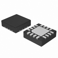
IC RCVR/DRVR RSECL SIGE DF 16QFN

NBSG16MMNG

Manufacturer Part Number
NBSG16MMNG
Description
IC RCVR/DRVR RSECL SIGE DF 16QFN
Manufacturer
ON Semiconductor
Type
Transceiverr
Datasheet

Specifications of NBSG16MMNG

Applications
Instrumentation
Mounting Type
Surface Mount
Package / Case
16-TFQFN Exposed Pad
Logic Family
NBSG
Logic Type
Receiver and Driver Translator Buffer
Supply Voltage (max)
- 3.465 V or 3.465 V
Supply Voltage (min)
- 2.375 V or 2.375 V
Maximum Operating Temperature
85 C
Mounting Style
SMD/SMT
Data Rate
10000 Mbps
Minimum Operating Temperature
- 40 C
Number Of Lines (input / Output)
/ /
Supply Current
51 mA
Lead Free Status / RoHS Status
Lead free / RoHS Compliant
Other names
NBSG16MMNGOS

Available stocks

Company
Part Number
Manufacturer
Quantity
Price
Part Number:
NBSG16MMNG
Manufacturer:
ON Semiconductor
Quantity:
135
Part Number:
NBSG16MMNG
Manufacturer:
ON/安森美
Quantity:
20 000
NBSG16M
2.5 V/3.3 V Multilevel Input
to CML Clock/Data
Receiver/Driver/Translator
Buffer
Description
receiver/driver/translator buffer. The device is functionally equivalent
to the EP16, LVEP16, or SG16 devices with CML output structure and
lower EMI capabilities.
LVNECL (Negative ECL), LVPECL (Positive ECL), LVTTL,
LVCMOS, CML, or LVDS. The CML output structure contains
internal 50 W source termination resistor to V
generates 400 mV output amplitude with 50 W receiver resistor to
V
device only. For all single−ended input conditions, the unused
complementary differential input is connected to V
reference voltage. V
used, decouple V
or sinking to 0.5 mA. When not used, V
Features
© Semiconductor Components Industries, LLC, 2009
March, 2009 − Rev. 7
CC
The NBSG16M is a differential current mode logic (CML)
Inputs incorporate internal 50 W termination resistors and accept
The V
V
Operating Range: V
50 W Receiver Resistor to V
Maximum Input Clock Frequency > 10 GHz Typical
Maximum Input Data Rate > 10 Gb/s Typical
120 ps Typical Propagation Delay
35 ps Typical Rise and Fall Times
Positive CML Output with Operating Range:
Negative CML Output with RSNECL or NECL Inputs with
CML Output Level; 400 mV Peak−to−Peak Output with
50 W Internal Input and Output Termination Resistors
Compatible with Existing 2.5 V/3.3 V LVEP, EP, LVEL
V
Pb−Free Packages are Available
and SG Devices
CC
BB
.
= 2.375 V to 3.465 V with V
Reference Voltage Output
BB
pin is internally generated voltage supply available to this
BB
via a 0.01 mF capacitor and limit current sourcing
BB
CC
may also rebias AC coupled inputs. When
= 0 V with V
CC
EE
EE
BB
= 0 V
= −2.375 V to −3.465 V
output should be left open.
BB
CC
. The device
as a switching
1
See detailed ordering and shipping information in the package
dimensions section on page 10 of this data sheet.
*For additional marking information, refer to
(Note: Microdot may be in either location)
Application Note AND8002/D.
MN SUFFIX
CASE 485G
QFN−16
A
L
Y
W
G
ORDERING INFORMATION
1
http://onsemi.com
= Assembly Location
= Wafer Lot
= Year
= Work Week
= Pb−Free Package
Publication Order Number:
1
16
DIAGRAM*
MARKING
ALYW G
16M
NBSG16M/D
SG
G

Related parts for NBSG16MMNG

NBSG16MMNG Summary of contents

Page 1

NBSG16M 2.5 V/3.3 V Multilevel Input to CML Clock/Data Receiver/Driver/Translator Buffer Description The NBSG16M is a differential current mode logic (CML) receiver/driver/translator buffer. The device is functionally equivalent to the EP16, LVEP16, or SG16 devices with CML output structure and lower ...

Page 2

Table 1. PIN DESCRIPTION Pin Name I − Á Á Á Á Á Á LVDS, CML, ECL, LVTTL, Á Á Á Á Á Á LVCMOS Input 3 D LVDS, CML, ECL, LVTTL, LVCMOS Input 4 ...

Page 3

V CC VTD VTD Figure 2. Logic Diagram Table 2. Interfacing Options INTERFACING OPTIONS CML LVDS AC−COUPLED RSECL, PECL, NECL LVTTL, LVCMOS Table 3. ATTRIBUTES Characteristics ESD Protection Moisture Sensitivity, ...

Page 4

Table 4. MAXIMUM RATINGS Symbol Parameter V Positive Power Supply CC V Negative Power Supply EE V Positive Input I Negative Input V Differential Input Voltage |D − D| INPP I Input Current Through R (50 W Resistor ...

Page 5

Table 5. DC CHARACTERISTICS, POSITIVE CML OUTPUT Symbol Characteristic I Positive Power Supply Current CC V Output HIGH Voltage (Note Output LOW Voltage (Note Input HIGH Voltage IH (Single−Ended) (Note 8) V Input LOW ...

Page 6

Table 6. DC CHARACTERISTICS, POSITIVE CML OUTPUT Symbol Characteristic I Positive Power Supply Current CC V Output HIGH Voltage (Note 10 Output LOW Voltage (Note Input HIGH Voltage IH (Single−Ended) (Note 11) V Input LOW ...

Page 7

Table 7. DC CHARACTERISTICS, NEGATIVE CML OUTPUT Symbol Characteristic I Positive Power Supply Current CC V Output HIGH Voltage (Note 13 Output LOW Voltage (Note 12 Input HIGH Voltage IH (Single−Ended) (Note 13) V Input LOW ...

Page 8

Table 8. AC CHARACTERISTICS V CC Symbol Characteristic V Output Voltage Amplitude OUTPP (See Figure 4) (Note 15 Propagation Delay to PLH t Output Differential PHL t Duty Cycle Skew (Note 16) SKEW t RMS Random Clock Jitter ...

Page 9

Application Information All inputs can accept PECL, CML, and LVDS signal levels. The input voltage can range from PECL Driver Recommended R Values 5.0 V 290 ...

Page 10

... Figure 9. Typical Termination for Output Driver and Device Evaluation (Refer to Application Note AND8020 − Termination of ECL Logic Devices) ORDERING INFORMATION Device NBSG16MMN NBSG16MMNG NBSG16MMNR2 NBSG16MMNR2G †For information on tape and reel specifications, including part orientation and tape sizes, please refer to our Tape and Reel Packaging Specifications Brochure, BRD8011/D. ...

Page 11

... Pb−Free strategy and soldering details, please download the ON Semiconductor Soldering and Mounting Techniques Reference Manual, SOLDERRM/D. N. American Technical Support: 800−282−9855 Toll Free USA/Canada Europe, Middle East and Africa Technical Support: Phone: 421 33 790 2910 Japan Customer Focus Center Phone: 81− ...

Related keywords