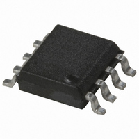
HCPL-0931 Avago Technologies US Inc., HCPL-0931 Datasheet - Page 14

HCPL-0931
Manufacturer Part Number
HCPL-0931
Description
ISOLATOR HS DIG DUAL BI 8-SOIC
Manufacturer
Avago Technologies US Inc.
Datasheet
1.HCPL-0900-000E.pdf
(14 pages)
Specifications of HCPL-0931
Inputs - Side 1/side 2
1/1
Number Of Channels
2
Isolation Rating
2500Vrms
Voltage - Supply
3 V ~ 5.5 V
Data Rate
100MBd
Propagation Delay
12ns
Output Type
CMOS
Package / Case
8-SOIC (3.9mm Width)
Operating Temperature
-40°C ~ 100°C
No. Of Channels
2
Isolation Voltage
2.5kV
Optocoupler Output Type
Logic Gate
Input Current
10µA
Output Voltage
5V
Opto Case Style
SOIC
No. Of Pins
8
Peak Reflow Compatible (260 C)
No
Input Current Max
10mA
Lead Free Status / RoHS Status
Contains lead / RoHS non-compliant
Propagation delay skew represents the uncertainty of
where an edge might be after being sent through a digital
isolator. Figure 5 shows that there will be uncertainty in
both the data and clock lines. It is important that these
two areas of uncertainty not overlap, otherwise the clock
signal might arrive before all of the data outputs have
settled, or some of the data outputs may start to change
before the clock signal has arrived. From these consider-
ations, the absolute minimum pulse width that can be
V
V
V
Figure 6. Timing Diagrams to Illustrate the Minimum Pulse Width, Rise and Fall Time, and Propagation Delay Enable to Output Waveforms for HCPL-9000
or HCPL-0900.
For product information and a complete list of distributors, please go to our web site:
Avago, Avago Technologies, and the A logo are trademarks of Avago Technologies in the United States and other countries.
Data subject to change. Copyright © 2005-2010 Avago Technologies. All rights reserved. Obsoletes 5989-0803EN
AV02-0137EN - July 14, 2010
t
t
t
IN
OUT
OE
PW
PLZ
PZH
50%
50%
Minimum Pulse Width
Propagation Delay, Low to High Impedance
Propagation Delay, High Impedance to High
t
PW
t
PLZ
t
PZH
t
t
t
t
PHZ
PZL
R
F
90%
www.avagotech.com
t
sent through digital isolators in a parallel application is
twice t
pulse width to ensure that any additional uncertainty in
the rest of the circuit does not cause a problem.
Figure 6 shows the minimum pulse width, rise and fall
time, and propagation delay enable to output waveforms
for HCPL-9000 or HCPL-0900.
F
Propagation Delay, High to High Impedance
Propagation Delay, High Impedance to Low
Rise Time
Fall Time
10%
PSK
. A cautious design should use a slightly longer
10%
90%
t
R
t
PHZ
t
PZL


