6N136-300E Avago Technologies US Inc., 6N136-300E Datasheet - Page 12
6N136-300E
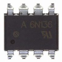
Manufacturer Part Number
6N136-300E
Description
OPTOCPLR TRANS-OUT 1MBD GW 8-SMD
Manufacturer
Avago Technologies US Inc.
Datasheet
1.HCPL-0500-000E.pdf
(17 pages)
Specifications of 6N136-300E
Input Type
DC
Package / Case
8-SMD Gull Wing
Voltage - Isolation
3750Vrms
Number Of Channels
1, Unidirectional
Current - Output / Channel
8mA
Data Rate
1Mbps
Propagation Delay High - Low @ If
200ns @ 16mA
Current - Dc Forward (if)
25mA
Output Type
Open Collector
Mounting Type
Surface Mount, Gull Wing
Isolation Voltage
3750 Vrms
Maximum Fall Time
0.8 us
Maximum Rise Time
0.8 us
Output Device
Transistor With Base
Configuration
1 Channel
Current Transfer Ratio
50 %
Maximum Baud Rate
1 MBps
Maximum Forward Diode Voltage
1.7 V
Maximum Reverse Diode Voltage
5 V
Maximum Input Diode Current
25 mA
Maximum Power Dissipation
100 mW
Maximum Operating Temperature
+ 100 C
Minimum Operating Temperature
- 55 C
No. Of Channels
1
Optocoupler Output Type
Phototransistor
Input Current
16mA
Output Voltage
15V
Opto Case Style
SMD
No. Of Pins
8
Ctr Max
50%
Ctr Min
15%
Rohs Compliant
Yes
Lead Free Status / RoHS Status
Lead free / RoHS Compliant
Lead Free Status / RoHS Status
Lead free / RoHS Compliant, Lead free / RoHS Compliant
Other names
516-1598-5
Available stocks
Company
Part Number
Manufacturer
Quantity
Price
Company:

Part Number:
6N136-300E
Manufacturer:
AVG
Quantity:
337
Part Number:
6N136-300E
Manufacturer:
AVAGO/安华高
Quantity:
20 000


Package Characteristics
Over recommended temperature (T
*All typicals at T
**The Input-Output Momentary Withstand Voltage is a dielectric voltage rating that should not be interpreted as an input-output continuous
voltage rating. For the continuous voltage rating refer to the IEC/EN/DIN EN 60747-5-2 Insulation Related Characteristics Table (if applicable), your
equipment level safety specification or Avago Application Note 1074 entitled “Optocoupler Input-Output Endurance Voltage, ” publication number
5963-2203E.
Notes:
10. The frequency at which the ac output voltage is 3 dB below its mid-frequency value.
11. The JEDEC registration for the 6N136 specifies a minimum CTR of 15%. Avago guarantees a minimum CTR of 19%.
12. See Option 020 data sheet for more information.
13. Use of a 0.1 µf bypass capacitor connected between pins 5 and 8 is recommended.
14. In accordance with UL 1577, each optocoupler is proof tested by applying an insulation test voltage ≥ 4500 V rms for 1 second (leakage
15. In accordance with UL 1577, each optocoupler is proof tested by applying an insulation test voltage ≥ 6000 V rms for 1 second (leakage
16. This rating is equally validated by an equivalent ac proof test.
12
1. Derate linearly above 70°C free-air temperature at a rate of 0.8 mA/°C (8-Pin DIP).
2. Derate linearly above 70°C free-air temperature at a rate of 1.6 mA/°C (8-Pin DIP).
3. Derate linearly above 70°C free-air temperature at a rate of 0.9 mW/°C (8-Pin DIP).
4. Derate linearly above 70°C free-air temperature at a rate of 2.0 mW/°C (8-Pin DIP).
5. CURRENT TRANSFER RATIO in percent is defined as the ratio of output collector current, I
6. Device considered a two-terminal device: Pins 1, 2, 3, and 4 shorted together and Pins 5, 6, 7, and 8 shorted together.
7. Common mode transient immunity in a Logic High level is the maximum tolerable (positive) dV
8. The 1.9 kΩ load represents 1 TTL unit load of 1.6 mA and the 5.6 kΩ pull-up resistor.
9. The 4.1 kΩ load represents 1 LSTTL unit load of 0.36 mA and 6.1 kΩ pull-up resistor.
Parameter
Input-Output
Momentary
Withstand
Voltage**
Input-Output
Resistance
Input-Output
Capacitance
Derate linearly above 85°C free-air temperature at a rate of 0.5 mA/°C (SO-8).
Derate linearly above 85°C free-air temperature at a rate of 1.0 mA/°C (SO-8).
Derate linearly above 85°C free-air temperature at a rate of 1.1 mW/°C (SO-8).
Derate linearly above 85°C free-air temperature at a rate of 2.3 mW/°C (SO-8).
mode pulse signal, V
Logic Low level is the maximum tolerable (negative) dV
output will remain in a Logic Low state (i.e., V
detection current limit, I
Related Characteristics Table if applicable.
detection current limit, I
Related Characteristics Table if applicable.
A
= 25°C.
CM
, to assure that the output will remain in a Logic High state (i.e., V
I-O
I-O
Sym.
V
R
C
I
≤ 5 µA). This test is performed before the 100% Production test shown in the IEC/EN/DIN EN 60747-5-2 Insulation
≤ 5 µA). This test is performed before the 100% Production test shown in the IEC/EN/DIN EN 60747-5-2 Insulation
I-O
ISO
I-O
I-O
(Option 020)
Widebody
Widebody
Widebody
8-Pin DIP
8-Pin DIP
8-Pin DIP
8-Pin DIP
8-Pin DIP
Device
SO-8
SO-8
SO-8
A
= 0°C to 70°C) unless otherwise specified.
O
< 0.8 V).
5000
CM
3750
5000
Min.
10
10
/dt on the trailing edge of the common mode pulse signal, V
12
11
Typ.*
10
10
0.6
0.5
12
13
Max.
0.6
1
O
V rms
Units
> 2.0 V). Common mode transient immunity in a
O
µA
pF
Ω
, to the forward LED input current, I
CM
Test Conditions
RH < 50%,
V
t = 1 min.,
T
45% RH, t = 5 s,
V
T
T
T
f = 1 MHz
/dt on the leading edge of the common
A
A
A
A
I-O
I-O
= 25°C
= 25°C
= 25°C
= 100°C
= 3 kVdc,
= 500 Vdc
CM
, to assure that the
Fig.
F
, times 100.
6, 15
6, 12,
6, 14
6, 16
Note
15
6
6
Related parts for 6N136-300E
Image
Part Number
Description
Manufacturer
Datasheet
Request
R

Part Number:
Description:
OPTOCOUPLER 1CH 1MBS 8-SMD GW
Manufacturer:
Avago Technologies US Inc.
Datasheet:

Part Number:
Description:
OPTOCOUPLER T-OUT 1MBD 8DIP
Manufacturer:
Avago Technologies US Inc.
Datasheet:
Part Number:
Description:
OPTOCOUPLER TRANS-OUT 1MBD 8DIP
Manufacturer:
Avago Technologies US Inc.
Datasheet:
Part Number:
Description:
OPTOCOUPLER 1CH 1MBS 8-SMD
Manufacturer:
Avago Technologies US Inc.
Datasheet:
Part Number:
Description:
OPTOCOUPLER 1CH 1MBS UL 8-SMD
Manufacturer:
Avago Technologies US Inc.
Datasheet:

Part Number:
Description:
OPTOCOUPLER 1CH 1MBS VDE 8-DIP
Manufacturer:
Avago Technologies US Inc.
Datasheet:
Part Number:
Description:
OPTOCOUPLER 1CH 1MBS UL 8-DIP
Manufacturer:
Avago Technologies US Inc.
Datasheet:
Part Number:
Description:
OPTOCOUPLER, TRANSISTOR, 3750VRMS
Manufacturer:
Avago Technologies US Inc.
Datasheet:

Part Number:
Description:
OPTOCOUPLER, TRANSISTOR, 3750VRMS
Manufacturer:
Avago Technologies US Inc.
Datasheet:
Part Number:
Description:
NPN-Output Dc-Input Optocoupler,1-CHANNEL,3.75kV ISOLATION,SO
Manufacturer:
Avago Technologies US Inc.
Datasheet:
Part Number:
Description:
Optocoupler(1MBd),IEC+LF
Manufacturer:
Avago Technologies US Inc.
Datasheet:
Part Number:
Description:
NPN-Output Dc-Input Optocoupler,1-CHANNEL,3.75kV ISOLATION,SO
Manufacturer:
Avago Technologies US Inc.
Datasheet:
Part Number:
Description:
Optocoupler
Manufacturer:
Avago Technologies US Inc.
Datasheet:
Part Number:
Description:
Optocoupler(1MBd),T/R+IEC+LF
Manufacturer:
Avago Technologies US Inc.
Datasheet:

Part Number:
Description:
OPTOCOUPLER GATE DRV 2A 16-SOIC
Manufacturer:
Avago Technologies US Inc.
Datasheet: