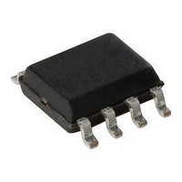
HCPL-T250-300E Avago Technologies US Inc., HCPL-T250-300E Datasheet - Page 5

HCPL-T250-300E
Manufacturer Part Number
HCPL-T250-300E
Description
OPTOCOUPLER DRIVER 1.5A 8-SMD GW
Manufacturer
Avago Technologies US Inc.
Datasheet
1.HCPL-T250-500E.pdf
(7 pages)
Specifications of HCPL-T250-300E
Voltage - Isolation
3750Vrms
Number Of Channels
1, Unidirectional
Current - Output / Channel
1.5A
Propagation Delay High - Low @ If
270ns @ 7mA ~ 16mA
Current - Dc Forward (if)
25mA
Input Type
DC
Output Type
Push-Pull, Totem-Pole
Mounting Type
Surface Mount, Gull Wing
Package / Case
8-SMD Gull Wing
No. Of Channels
1
Optocoupler Output Type
Gate Drive
Input Current
16mA
Output Voltage
30V
Opto Case Style
SMD
No. Of Pins
8
Peak Reflow Compatible (260 C)
Yes
Isolation Voltage
3.75kV
Number Of Elements
1
Forward Voltage
1.8V
Forward Current
20mA
Package Type
PDIP SMD
Operating Temp Range
-20C to 85C
Power Dissipation
250mW
Propagation Delay Time
500ns
Pin Count
8
Mounting
Surface Mount
Reverse Breakdown Voltage
5V
Operating Temperature Classification
Commercial
Lead Free Status / RoHS Status
Lead free / RoHS Compliant
Lead Free Status / RoHS Status
Lead free / RoHS Compliant, Lead free / RoHS Compliant
Available stocks
Company
Part Number
Manufacturer
Quantity
Price
Company:
Part Number:
HCPL-T250-300E
Manufacturer:
AVAGO
Quantity:
45 000
Part Number:
HCPL-T250-300E
Manufacturer:
AVAGO/安华高
Quantity:
20 000
Regulatory Information
The HCPL‑T250 has been approved by the following organizations:
UL
Recognized under UL 1577, Component Recognition
Program, File E55361.
CSA
Approved under CSA Component Acceptance Notice
#5, File CA 88324.
Insulation and Safety Related
Absolute Maximum Ratings
Notes:
1. Maximum pulse width = 10 µs, maximum duty cycle = 0.2%. See HCPL‑3120 Applications section for additional details on limiting I
2. Derate linearly above 70°C free‑air temperature at a rate of 0.3 mA/°C.
3. Derate lineraly above 70°C free‑air temperature at a rate of 4.8 mW/°C.
Minimum External Air Gap
(Clearance)
Minimum External Tracking
(Creepage)
Minimum Internal Plastic Gap
(Internal Clearance)
Tracking Resistance
(Comparative Tracking Index)
Isolation Group
Operating Temperature
“High” Peak Output Current
“High” Peak Output Current
Storage Temperature
Average Input Current
Peak Transient Input Current
(<1 µs Pulse Width, 300 pps)
Reverse Input Voltage
Supply Voltage
Output Voltage
Output Power Dissipation
Lead Solder Temperature
Solder Reflow Temperature Profile
Parameter
Parameter
(Compared with HCPL‑3120)
Symbol
L(101)
L(102)
CTI
(V
I
I
OH(PEAK)
I
OL(PEAK)
Symbol
I
F(TRAN)
CC
F(AVG)
≥175
Value
0.08
V
P
T
T
V
7.1
7.4
IIIa
‑ V
A
O
O
R
S
EE
)
260°C for 10 sec., 1.6 mm below seating plane
Volts
Units
mm
mm
mm
Units
IEC/EN/DIN EN 60747-5-2
Approved under:
IEC 60747‑5‑2:1997 + A1:2002
EN 60747‑5‑2:2001 + A1:2002
DIN EN 60747‑5‑2 (VDE 0884 Teil 2):2003‑01.
(Option 060 only)
mW
mA
°C
°C
See Package Outline Drawings section
A
A
A
V
V
V
Measured from input terminals to
output terminals, shortest distance through
air.
Measured from input terminals to
output terminals, shortest distance path
along body.
Insulation thickness between emitter
and detector; also known as distance
through insulation
DIN IEC 112/VDE 0303 Part 1
Material Group (DIN VDE 0110, 1/89, Table 1)
Min.
‑ 40
‑55
0
0
HCPL-3120
Max.
100
125
V
250
2.5
2.5
1.0
Conditions
25
35
5
CC
Min.
‑20
‑55
0
0
HCPL-T250
Max.
125
250
V
1.5
1.5
1.0
85
20
35
5
CC
OH(PEAK)
Note
2
3
1
.


