HCPL-0454 Avago Technologies US Inc., HCPL-0454 Datasheet
HCPL-0454
Specifications of HCPL-0454
Available stocks


Related parts for HCPL-0454


HCPL-0454 Summary of contents
Page 1
... RoHS 6 fully compliant options available; -xxxE denotes a lead-free product Description The HCPL-4504 and HCPL-0454 contain a GaAsP LED while the HCPL-J454 and HCNW4504 contain an AlGaAs LED. The LED is optically coupled to an integrated high gain photo detector. The HCPL-4504 series has short propagation delays and high CTR. The HCPL-4504 series also has a guaranteed propagation delay diff ...
Page 2
... Ordering Information HCPL-0454, HCPL-4504 and HCPL-J454 are UL Recognized with 3750 Vrms for 1 minute per UL1577. HCNW4504 is UL Recognized with 5000 Vrms for 1 minute per UL1577. HCPL-0454, HCPL-4504, HCPL-J454 and HCNW4504 are approved under CSA Component Acceptance Notice #5, File CA 88324. Option Part ...
Page 3
... TYPE NUMBER A XXXXZ R U YYWW 1.19 (0.047) MAX. 3.56 ± 0.13 (0.140 ± 0.005) 1.080 ± 0.320 (0.043 ± 0.013) HCPL-4504 Gull Wing Surface Mount Option 300 Outline Drawing 9.65 ± 0.25 (0.380 ± 0.010 1.19 (0.047) MAX. 1.080 ± 0.320 (0.043 ± ...
Page 4
... TYPE NUMBER A XXXX R U YYWW 1.19 (0.047) MAX. 3.56 ± 0.13 (0.140 ± 0.005) 1.080 ± 0.320 (0.043 ± 0.013) HCPL-J454 Gull Wing Surface Mount Option 300 Outline Drawing 9.80 ± 0.25 (0.386 ± 0.010 1.19 (0.047) MAX. 1.080 ± 0.320 (0.043 ± ...
Page 5
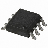
... MAX. [1.080] 0.320 0.043 0.013 0.100 DIMENSIONS IN [MILLIMETERS] INCHES OPTION NUMBERS 400 AND 600 NOT MARKED. NOTE: FLOATING LEAD PROTRUSION IS 0.5 mm (20 mils) MAX. HCPL-0454 Outline Drawing (8-Pin Small Outline Package XXX 3.937 ± 0.127 YWW (0.155 ± 0.005) ...
Page 6
HCNW4504 Outline Drawing (8-Pin Widebody Package) 11.15 ± 0.15 (0.442 ± 0.006 HCNWXXXX YYWW 2.54 (0.100) TYP. 1.78 ± 0.15 (0.070 ± 0.006) HCNW4504 Gull Wing Surface Mount Option 300 Outline Drawing 11.15 ...
Page 7
Solder Refl ow Temperature Profi le 300 PREHEATING RATE 3 ° °C/–0.5 °C/SEC. REFLOW HEATING RATE 2.5 °C ± 0.5 °C/SEC. 200 160 °C 150 °C 140 °C 3 ° °C/–0.5 °C 100 ROOM TEMPERATURE 0 ...
Page 8
... Creepage and clear- ance distances will also change depending on factors such as pollution degree and insulation level. HCPL-0454 HCNW4504 3750 Vrms / 5000 Vrms / 1 minute ...
Page 9
... NOTE: These optocouplers are suitable for "safe electrical isolation" only within the safety limit data. Maintenance of the safety data shall be ensured by means of protective circuits. NOTE: Insulation Characteristics are per IEC/EN/DIN EN 60747-5-2. NOTE: Surface mount classifi cation is Class A in accordance with CECC 00802. 9 HCPL-0454 HCPL-4504 Symbol OPTION 060 OPTION 060 ...
Page 10
... HCPL-0454 HCPL-J454 HCNW4504 -55 I F(AVG) I HCPL-4504 F(PEAK) HCPL-0454 HCPL-J454 HCNW4504 I HCPL-4504 F(TRANS) HCPL-0454 HCPL-J454 HCNW4504 V HCPL-4504 R HCPL-0454 HCPL-J454 HCNW4504 P HCPL-4504 IN HCPL-0454 HCPL-J454 HCNW4504 I O(AVG) I O(PEAK HCPL-4504 LS HCPL-J454 HCNW4504 T HCPL-0454, See Package Outline Drawings RP Option 300 , Option 500, Option 400E & Option 600E. ...
Page 11
... Supply HCPL-0454 Current HCNW4504 HCPL-J454 Logic High I CCH Supply Current Input Forward V HCPL-4504 F Voltage HCPL-0454 HCPL-J454 HCNW4504 Input Reverse BV HCPL-4504 R Breakdown HCPL-0454 Voltage HCPL-J454 HCNW4504 Temperature ∆V HCPL-4504 F Coeffi cient HCPL-0454 ∆ Forward HCPL-J454 Voltage HCNW4504 Input C HCPL-4504 IN Capacitance HCPL-0454 ...
Page 12
... PLH Diff erence Be- t PHL tween Any 2 Parts Common Mode | Transient Immu- nity at Logic High | Level Output | Common Mode Transient Immu- |CM | HCPL- L nity at Logic Low J454 Level Output Others 10 | *All typicals 25° Min. Typ. Max. Units Test Conditions 0.2 0.3 μ 25° ...
Page 13
... HCPL-J454 HCNW4504 Capacitance C HCPL-4504 I-O (Input-Output) HCPL-0454 HCPL-J454 HCNW4504 All typicals 25°C.. A †The Input-Output Momentary Withstand Voltage is a dielectric voltage rating that should not be interpreted as an input-output continuous voltage rating. For the continuous voltage rating refer to the IEC/EN/DIN EN 60747-5-2 Insulation Related Characteristics Table (if applicable), your equipment level safety specifi ...
Page 14
... V – FORWARD VOLTAGE – VOLTS F Figure 3. Input current vs. forward voltage. 14 HCPL-J454 25° 5 – OUTPUT VOLTAGE – HCPL-J454 2.0 NORMALIZED 25° 1.0 0 – INPUT CURRENT – HCPL-J454/HCNW4504 1000 T = 25°C A 100 – 1.0 0.1 ...
Page 15
... V V THHL THLH PHL PLH Figure 6. Switching test circuit 90% 90 10% 10 SWITCH SWITCH mA Figure 7. Test circuit for transient immunity and typical waveforms. 15 HCPL-J454 1.05 NORMALIZED 25° 0.95 0.9 0.85 -60 -40 - 100 T – TEMPERATURE – ° PULSE F 1 GEN Ω ...
Page 16
... 1.5 V THHL THLH 1.0 10% DUTY CYCLE t PLH 0.8 0 PHL 0 0.2 0 – LOAD RESISTANCE – kΩ L Figure 9. Propagation delay time vs. load resis- tance. HCPL-J454/HCNW4504 1 15 kΩ 1 100 1.5 V THHL t PLH V = 2.0 V THLH 0.8 50% DUTY CYCLE 0.7 0.6 0.5 t PHL 0.4 0.3 ...
Page 17
... LED Figure 16. Typical power inverter. 17 HCPL-0454 OPTION 060/HCNW4504 1000 P (mW) for HCNW4504 S 900 I (mA) for HCNW4504 S P (mW) for HCPL-0454 S 800 OPTION 060 I (mA) for HCPL-0454 700 S OPTION 060 600 500 400 300 200 (150) 100 100 125 150 175 T – CASE TEMPERATURE – °C ...
Page 18
... Figure 17. LED delay and dead time diagram. Power Inverter Dead Time and Propagation Delay Specifi ca- tions The HCPL-4504/0454/J454 and HCNW4504 include a specifi ca tion intended to help designers minimize “dead time” in their power inverter designs. The new “propaga- tion delay diff erence” specifi cation (t deter min ing not only how much optocoupler switch- ing delay is needed to prevent “ ...
Page 19
... Therefore, opto coup lers with tight propagation delay specifi cations (and not just shorter delays or lower pulse- width distortion) can achieve short dead times in power inverters. The HCPL-4504/0454/J454 and HCNW4504 specify a minimum (t ing temperature range of 0-70°C, resulting in a maximum dead time of 2.0 μ ...