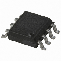
HCPL-0738-000E Avago Technologies US Inc., HCPL-0738-000E Datasheet - Page 4

HCPL-0738-000E
Manufacturer Part Number
HCPL-0738-000E
Description
OPTOCOUPLER CMOS 15MBD 8SOIC
Manufacturer
Avago Technologies US Inc.
Datasheet
1.HCPL-0738-500.pdf
(8 pages)
Specifications of HCPL-0738-000E
Package / Case
8-SOIC (0.154", 3.90mm Width)
Voltage - Isolation
3750Vrms
Number Of Channels
2, Unidirectional
Current - Output / Channel
2mA
Data Rate
15MBd
Propagation Delay High - Low @ If
35ns @ 12mA
Current - Dc Forward (if)
20mA
Input Type
DC
Output Type
Open Collector
Mounting Type
Surface Mount
Isolation Voltage
3750 Vrms
Maximum Continuous Output Current
2 mA
Maximum Fall Time
0.025 us
Maximum Forward Diode Current
20 mA
Minimum Forward Diode Voltage
1.3 V
Output Device
Logic Gate Photo IC
Configuration
2 Channel
Maximum Baud Rate
15 MBd(Typ)
Maximum Forward Diode Voltage
1.8 V
Maximum Operating Temperature
+ 100 C
Minimum Operating Temperature
- 40 C
No. Of Channels
2
Optocoupler Output Type
Logic Gate
Input Current
16mA
Output Voltage
5V
Opto Case Style
SOIC
No. Of Pins
8
Common Mode Ratio
10000
Rohs Compliant
Yes
Lead Free Status / RoHS Status
Lead free / RoHS Compliant
Lead Free Status / RoHS Status
Lead free / RoHS Compliant, Lead free / RoHS Compliant
Other names
516-1536-5
Regulatory Information
The HCPL-0738 has been
approved by the following
organizations:
UL
Recognized under UL 1577,
component recognition program,
File E55361.
Insulation and Safety Related Specifications (approval pending)
Parameter
Minimum External Air Gap
(Clearance)
Minimum External Tracking
(Creepage)
Minimum Internal Plastic Gap
(Internal Clearance)
Tracking Resistance
(Comparative Tracking Index)
Isolation Group
Absolute Maximum Ratings
Parameter
Storage Temperature
Ambient Operating Temperature
Supply Voltage
Output Voltage
Average Forward Input Current
Average Output Current
Lead Solder Temperature
Solder Reflow Temperature Profile
Recommended Operating Conditions
Parameter
Ambient Operating Temperature
Supply Voltages
Input Current (ON)
All Avago data sheets report the creepage and clearance
inherent to the optocoupler component itself. These
dimensions are needed as a starting point for the equip-
ment designer when determining the circuit insulation
requirements. However, once mounted on a printed
circuit board, minimum creepage and clearance require-
ments must be met as specified for individual equipment
standards. For creepage, the shortest distance path along
Symbol
L(I01)
L(I0)
CTI
Symbol
T
T
V
V
I
I
60˚C for 10 seconds, 1.6 mm below seating plane
See Solder Reflow Thermal Profile section
Symbol
T
V
I
F
O
F
A
A
S
DD
O
DD
Value
.9
.8
0.08
≥ 175
IIIa
Units
mm
mm
mm
Volts
EN 60747-5-2:2001 + A1:2002
CSA
Approved under CSA Component
Acceptance Notice #5, File
CA88324.
IEC/EN/DIN EN 60747-5-2
Approved under:
IEC 60747-5-2:1997 + A1:2002
DIN EN 60747-5-2 (VDE 0884 Teil 2):2003-01
(Option 060 only)
Conditions
Measured from input terminals to output terminals,
shortest distance through air.
Measured from input terminals to output terminals,
shortest distance path along body.
Insulation thickness between emitter and detector; also
known as distance through insulation.
DIN IEC 11/VDE 0303 Part 1
Material Group (DIN VDE 0110, 1/89, Table 1)
the surface of a printed circuit board between the solder
fillets of the input and output leads must be considered.
There are recommended techniques such as grooves
and ribs which may be used on a printed circuit board
to achieve desired creepage and clearances. Creepage
and clearance distances will also change depending on
factors such as pollution degree and insulation level.
Minimum
–55
–0
0
–0.5
—
—
Minimum
–0
.5
10
Maximum
15
100
6.0
V
0
Maximum
100
5.5
16
DD
+ 0.5
Units
˚C
˚C
Volts
Volts
mA
mA
Units
˚C
V
mA


