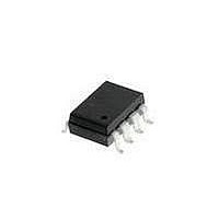
HCPL-5201#300 Avago Technologies US Inc., HCPL-5201#300 Datasheet

HCPL-5201#300
Specifications of HCPL-5201#300
Available stocks
Related parts for HCPL-5201#300
HCPL-5201#300 Summary of contents
Page 1
Hermetically Sealed Low IF, Wide VCC, Logic Gate Optocouplers Data Sheet Description �he�e unit� are �ingle�� dual and quad channel�� hermeti� call�� �ealed o�tocou�ler�. �he �roduct� are ca�able o� o�eration and �torage over the �ull militar�� tem�erature range and can be �urcha�ed a� either �tandard �roduct or with �ull M���P��������� Cla�� �evel �� or � te�ting or �rom the a��ro�riate DSCC ...
Page 2
Functional Diagram Multi�le Channel Device� �vailable GND Package �t��le� �or the�e �art� are � �in D�P through hole (ca�e outline P)�� �6 �in D�P flat �ack (ca�e outline �)�� and leadle�� ceramic chi� carrier (ca�e outline �). Device� ma�� be �urcha�ed with a variet�� o� lead bend and �lating o�tion��� �ee Selection �uide �able �or detail�. Standard Microcircuit Drawing (SMD) �art� are available �or each �ackage and lead �t��le. Becau�e the �ame electrical die (emitter� and detector�) are u�ed �or each channel o� each device li�ted in thi� data �heet�� ...
Page 3
... Pin Flat Pack 20 Pad LCCC Unformed Leads Surface Mount GND None CC HCPL-6250 HCPL-6230 HCPL-6251 HCPL-6231 HCPL-625K HCPL-623K Gold Plate Solder Pads * 5962- 5962- 8876903FX 88769022X 8876903FC 88769022A 5962- 5962- 8876906KFX 8876905K2X 8876906KFC 8876905K2A ...
Page 4
Outline Drawings 8 Pin DIP Through Hole, 1 and 2 Channel 9.40 (0.370) 9.91 (0.390) 0.76 (0.030) 1.27 (0.050) 0.51 (0.020) MIN. 2.29 (0.090) 0.51 (0.020) 2.79 (0.110) NOTE: DIMENSIONS IN MILLIMETERS (INCHES). 16 Pin Flat Pack, 4 Channels 11.13 ...
Page 5
Terminal LCCC Surface Mount, 2 Channels 8.70 (0.342) 9.10 (0.358) 4.95 (0.195) 5.21 (0.205) 1.78 (0.070) 2.03 (0.080) 8.70 (0.342) 9.10 (0.358) 4.95 (0.195) 5.21 (0.205) 1.78 (0.070) 2.03 (0.080) 0.64 (0.025) (20 PLCS) 1.52 (0.060) 2.03 (0.080) NOTE: ...
Page 6
Hermetic Optocoupler Options Option Description 100 Surface mountable hermetic optocoupler with leads trimmed for butt joint assembly. This option is available on commercial and hi-rel product in 8 pin DIP (see drawings below for details). 0.51 (0.020) MIN. 2.29 (0.090) ...
Page 7
Absolute Maximum Ratings Parameter Storage �em�erature �ange ��erating �mbient �em�erature Junction �em�erature Ca�e �em�erature �ead Solder �em�erature (�.6 mm below �eating �lane) �verage �orward Current�� each channel Peak �n�ut Current�� each channel �ever�e �n�ut �oltage�� each channel �verage �ut�ut Current�� each channel Su��l�� �oltage �ut�ut �oltage�� each channel Package Power Di��i�ation�� each channel Single Channel Product Only �ri�State Enable �oltage 8 Pin Ceramic DIP Single Channel Schematic Note enable �in 6. �n e�ternal 0.0� �� to 0.� �� b���a�� ca�acitor i� recommended between � ESD Classification (MIL-STD-883, Method 3015) ��CP����00�0��0� and ��CP��6��0������ ��CP�����0������ and ��CP��6��0������ Recommended Operating Conditions ...
Page 8
Electrical Characteristics � = ����C to �����C�� ��.� � ≤ � ≤ �0 ��� � m� ≤ � � CC Parameter Symbol �ogic �ow �ut�ut �oltage � �� �ogic ��igh �ut�ut �oltage � ��� �ut�ut �eakage � ����� Current (� �� � ) �U� CC �ogic Single � CC� �ow Channel Su��l�� Current Dual Channel �uad Channel �ogic Single � CC�� ��igh ...
Page 9
Electrical Characteristics - Single Channel Product Only � = ����C to �����C�� ��.� � ≤ � ≤ �0 ��� � m� ≤ � � CC unle�� otherwi�e ��ecified. Group A, Parameter Symbol Sub-groups ��igh �m�edance � ������� �Z� State �ut�ut Current � ������� �Z�� �ogic ��igh � ��� ��� � E�� Enable �oltage �ogic �ow � ��� ��� � E� Enable �oltage �ogic ��igh ...
Page 10
Typical Characteristics �ll t���ical value� are at � = ���C�� � � Parameter �n�ut Current �����tere�i� �n�ut Diode �em�erature Coefficient �e�i�tance (�n�ut��ut�ut) Ca�acitance (�n�ut��ut�ut) �n�ut Ca�acitance �ut�ut �i�e �ime (�0�90%) �ut�ut �all �ime (90��0%) Single Channel Product Only �ut�ut Enable �ime to �ogic ��igh �ut�ut Enable �ime to �ogic �ow �ut�ut Di�able �ime �rom �ogic ��igh �ut�ut Di�able �ime �rom �ogic �ow Multi-Channel Product Only �n�ut��n�ut �n�ulation �eakage Current �e�i�tance (�n�ut��n�ut) Ca�acitance (�n�ut��n�ut) Note��� �. Peak �orward �n�ut Current �ul�e width < �0 �� at � ���z ma�imum re�etition rate. �. Each channel o� a multichannel device. �. Duration o� out�ut �hort circuit time not to e�ceed �0 m�. ��. �ll device� are con�idered two�terminal device��� mea�ured between all in�ut lead� or terminal� �horted together and all out�ut lead� or ter� minal� �horted together. �. ...
Page 11
Figure 1. Typical Logic Low Output Voltage vs. Temperature. Figure 3. Output Voltage vs. Forward Input Current PULSE GEN. OUTPUT MONITORING 100 kHz NODE D.U. ...
Page 12
Figure 6. Typical Propagation Delay vs. Temperature INCLUDING PROBE PULSE AND JIG CAPACITANCE. GENERATOR Ω D.U. ...
Page 13
V CC1 (+5 V) 665 Ω D.U. DATA INPUT TTL OR LSTTL V E GND TOTEM V R POLE CC2 L OUTPUT GATE 3.83 K ...
Page 14
D.U.T 100 Ω 1.90 V CONDITIONS - +125 ˚C A *ALL CHANNELS TESTED SIMULTANEOUSLY. Figure 14. Single Channel Operating Circuit for Burn-in and Steady ...


