PC410L0NIT0F Sharp Microelectronics, PC410L0NIT0F Datasheet
PC410L0NIT0F
Specifications of PC410L0NIT0F


Related parts for PC410L0NIT0F


PC410L0NIT0F Summary of contents
Page 1
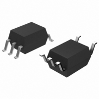
PC410L0NIP0F Series ■ Description PC410L0NIP0F Series contains a LED optically cou- pled to an OPIC chip packaged pin mini-flat. Input-output isolation voltage(rms) is 3.75 kV. High speed response(TYP. 10 Mb/s) and CMR is MIN. 10 ...
Page 2
Internal Connection Diagram 1 3 ■ Outline Dimensions 1. Mini-flat Package [ex. PC410L0NIP0F] ±0.3 3.6 ±0.25 ±0.25 1.27 1. SHARP mark "S" PC4 1 0L Anode mark Date code 1 3 ±0.1 0.4 Factory identification mark ...
Page 3
Date code (2 digit) 1st digit Year of production A.D. Mark A.D Mark 1990 A 2002 P 1991 B 2003 R 1992 C 2004 S 1993 D 2005 T 1994 E 2006 U 1995 F 2007 V 1996 H 2008 ...
Page 4
Absolute Maximum Ratings Parameter Symbol Forward current I F Reverse voltage V R Power dissipation P Supply voltage V CC High level output voltage V OH Low level output current I OL Collector power dissipation P C Operating temperature ...
Page 5
Model Line-up Taping Package 3 000pcs/reel DIN EN60747-5-2 −−−−−− Model No. PC410L0NIP0F PC410L0YIP0F Please contact a local SHARP sales representative to inquire about production status. Approved 5 PC410L0NIP0F Series Sheet No.: D2-A04802EN ...
Page 6
Fig.1 Test Circuit for Propagation Delay Time and Rise Time, Fall Time I F Pulse input 1 3 47Ω Fig.2 Test Circuit for Instantaneous Common Mode Rejection Voltage ...
Page 7
Fig.5 Forward Current vs. Forward Voltage 100 T =25˚ =50˚ =85˚ 0.1 1 1.2 1.4 1.6 Forward voltage V Fig.7 Low Level Output Voltage vs. Ambient Temperature 0.8 0.6 I =16.0mA O I ...
Page 8
Fig.11 Propagation Delay Time vs. Ambient Temperature 100 PLH 40 t PHL 20 0 −40 − Ambient temperature T Remarks : Please be aware that all data in the graph are just for reference and ...
Page 9
Design Considerations ● Recommended operating conditions Parameter Symbol I Low level input current I High level input current V Supply voltage Fan out (TTL load) Operating temperature T ● Notes about static electricity Transistor of detector side in bipolar ...
Page 10
Manufacturing Guidelines ● Soldering Method Reflow Soldering: Reflow soldering should follow the temperature profile shown below. Soldering should not exceed the curve of temperature profile and time. Please don't solder more than twice. (˚C) 300 Terminal : 260˚C peak ...
Page 11
Cleaning instructions Solvent cleaning: Solvent temperature should be 45˚C or below Immersion time should be 3 minutes or less Ultrasonic cleaning: The impact on the device varies depending on the size of the cleaning bath, ultrasonic output, cleaning time, ...
Page 12
Package specification ● Tape and Reel package Package materials Carrier tape : A-PET (with anti-static material) Cover tape : PET (three layer system) Reel : PS Carrier tape structure and Dimensions F Dimensions List A ±0.3 12.0 H ±0.1 ...
Page 13
Important Notices · The circuit application examples in this publication are provided to explain representative applications of SHARP devices and are not intended to guarantee any circuit design or license any intellectual property rights. SHARP takes no responsibility for ...