TLP620(F,T) Toshiba, TLP620(F,T) Datasheet - Page 2
TLP620(F,T)
Manufacturer Part Number
TLP620(F,T)
Description
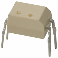
PHOTOCPLR AC IN TRANS-OUT 4-DIP
Manufacturer
Toshiba
Specifications of TLP620(F,T)
Number Of Channels
1
Input Type
AC, DC
Voltage - Isolation
5000Vrms
Current Transfer Ratio (min)
50% @ ±5mA
Current Transfer Ratio (max)
600% @ ±5mA
Voltage - Output
55V
Current - Output / Channel
50mA
Current - Dc Forward (if)
60mA
Vce Saturation (max)
400mV
Output Type
Transistor
Mounting Type
Through Hole
Package / Case
4-DIP (0.300", 7.62mm)
Output Device
Transistor
Number Of Elements
1
Forward Voltage
1.3V
Forward Current
60mA
Collector-emitter Voltage
55V
Package Type
PDIP
Collector Current (dc) (max)
50mA
Isolation Voltage
5000Vrms
Power Dissipation
250mW
Current Transfer Ratio
600%
Pin Count
4
Mounting
Through Hole
Operating Temp Range
-25C to 85C
Operating Temperature Classification
Commercial
Maximum Collector Emitter Voltage
55 V
Maximum Collector Emitter Saturation Voltage
0.4 V
Maximum Forward Diode Voltage
1.3 V
Maximum Collector Current
50 mA
Maximum Power Dissipation
250 mW
Maximum Operating Temperature
+ 100 C
Minimum Operating Temperature
- 55 C
Maximum Fall Time
3 us
Maximum Input Diode Current
60 mA
Maximum Rise Time
2 us
Lead Free Status / RoHS Status
Lead free / RoHS Compliant
Other names
TLP620F


•
•
•
Absolute Maximum Ratings
Isolation voltage: 5000V
Option (D4) type
VDE approved: DIN EN 60747-5-2, certificate no.40009302
Creepage distance: 6.4mm (min.)
Clearance: 6.4mm (min.)
Insulation thickness: 0.4mm (min.)
Storage temperature range
Operating temperature range
Lead soldering temperature
Total package power dissipation
Total package power dissipation
derating (Ta ≥ 25°C, 1 circuit)
Isolation voltage
Note: Using continuously under heavy loads (e.g. the application of high temperature/current/voltage and the
UL recognized
BSI approved
Forward current
Forward current derating
Pulse forward current
Power dissipation (1 circuit)
Power dissipation derating
Junction temperature
Collector−emitter voltage
Emitter−collector voltage
Collector current
Collector power dissipation
(1 circuit)
Collector power dissipation
derating (1 circuit) (Ta ≥ 25°C)
Junction temperature
(Note) When an EN 60747-5-2 approved type is needed,
*1 UL1577
*2 BS EN60065: 2002, BS EN60950-1: 2002
Maximum operating insulation voltage: 890V
Highest permissible over voltage: 8000V
significant change in temperature, etc.) may cause this product to decrease in the reliability significantly even
if the operating conditions (i.e. operating temperature/current/voltage, etc.) are within the absolute maximum
ratings.
Please design the appropriate reliability upon reviewing the Toshiba Semiconductor Reliability Handbook
(“Handling Precautions”/“Derating Concept and Methods”) and individual reliability data (i.e. reliability test
report and estimated failure rate, etc).
please designate the “Option(D4)”.
Characteristic
E67349
7426, 7427
rms
Made In Japan
(min.)
(Ta = 25°C)
ΔP
ΔP
ΔP
I
ΔI
Symbol
F (RMS)
V
V
T
T
BV
T
F
I
P
P
D
CEO
ECO
C
P
sold
T
I
FP
T
T
opr
stg
C
/ °C
D
C
T
/ °C
j
/ °C
j
/ °C
S
*1
*2
PK
E152349
7426, 7427
PK
Made In Thailand
2
−0.7 (Ta ≥ 39°C)
TLP620
−1.0
−1.5
−2.5
100
150
250
60
5000 (AC, 1 min., RH ≤ 60%)
1 (100μs pulse, 100pps)
TLP620,TLP620−2,TLP620−4
*1
*2
260 (10s)
−55~125
−55~100
Rating
125
125
55
50
7
−0.5 (Ta ≥ 25°C)
TLP620−2
TLP620−4
−0.7
−1.0
−1.5
100
150
50
70
2007-10-01
mW / °C
mW / °C
mW / °C
mA / °C
V
Unit
mW
mW
mW
mA
mA
°C
°C
°C
°C
°C
A
V
V
rms
Related parts for TLP620(F,T)
Image
Part Number
Description
Manufacturer
Datasheet
Request
R

Part Number:
Description:
PHOTOCPLR DL AC IN TRANSOUT 8DIP
Manufacturer:
Toshiba
Datasheet:

Part Number:
Description:
Manufacturer:
TOSHIBA Semiconductor CORPORATION
Datasheet:

Part Number:
Description:
PHOTOCPLR QD AC IN TRANOUT 16DIP
Manufacturer:
Toshiba
Datasheet: