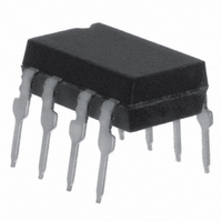
ILD74 Vishay, ILD74 Datasheet - Page 2

ILD74
Manufacturer Part Number
ILD74
Description
OPTOCPLR PHOTOTRAN 2CH 35% 8DIP
Manufacturer
Vishay
Specifications of ILD74
Mounting Type
Through Hole
Isolation Voltage
5300 Vrms
Number Of Channels
2
Input Type
DC
Voltage - Isolation
5300Vrms
Voltage - Output
20V
Current - Dc Forward (if)
60mA
Vce Saturation (max)
500V
Output Type
Transistor
Package / Case
8-DIP (0.300", 7.62mm)
Maximum Input Diode Current
60 mA
Output Device
Transistor
Configuration
2
Maximum Collector Emitter Voltage
20 V
Maximum Collector Emitter Saturation Voltage
500 mV
Current Transfer Ratio
35 % (Typ)
Maximum Forward Diode Voltage
1.5 V
Maximum Power Dissipation
400 mW
Maximum Operating Temperature
+ 100 C
Minimum Operating Temperature
- 55 C
No. Of Channels
2
Optocoupler Output Type
Phototransistor
Input Current
20mA
Output Voltage
20V
Opto Case Style
DIP
No. Of Pins
8
Approval Bodies
UL
Rohs Compliant
Yes
Number Of Elements
2
Forward Voltage
1.5V
Forward Current
60mA
Collector-emitter Voltage
20V
Package Type
PDIP
Power Dissipation
400mW
Collector-emitter Saturation Voltage
0.5V
Pin Count
8
Mounting
Through Hole
Operating Temp Range
-55C to 100C
Operating Temperature Classification
Industrial
Lead Free Status / RoHS Status
Lead free / RoHS Compliant
Current - Output / Channel
-
Current Transfer Ratio (max)
-
Current Transfer Ratio (min)
-
Lead Free Status / Rohs Status
Lead free / RoHS Compliant
Other names
751-1326-5
ILD74GI
ILD74GI
ILD74GI
ILD74GI
Available stocks
Company
Part Number
Manufacturer
Quantity
Price
Part Number:
ILD74
Manufacturer:
SIEMENS/西门子
Quantity:
20 000
IL74/ ILD74/ ILQ74
Vishay Semiconductors
Absolute Maximum Ratings
T
Stresses in excess of the absolute Maximum Ratings can cause permanent damage to the device. Functional operation of the device is
not implied at these or any other conditions in excess of those given in the operational sections of this document. Exposure to absolute
Maximum Rating for extended periods of the time can adversely affect reliability.
Input
(each channel)
Output
Coupler
www.vishay.com
2
Peak reverse voltage
Forward continuous current
Power dissipation
Derate linearly from 55 %
Collector-emitter breakdown voltage
Emitter-collector breakdown voltage
Collector-base breakdown voltage
Power dissipation
Derate linearly from 25 °C
Isolation test voltage
Isolation resistance
Total package dissipation
Derate linearly from 25 °C
Creepage
Clearance
Storage temperature
Operating temperature
Lead soldering time at 260 °C
amb
= 25 °C, unless otherwise specified
Parameter
Parameter
Parameter
t = 1.0 sec.
V
V
IO
IO
= 500 V, T
= 500 V, T
Test condition
Test condition
A
A
Test condition
= 25 °C
= 100 °C
ILQ74
ILQ74
ILD74
ILD74
Part
IL74
IL74
Symbol
Symbol
BV
BV
BV
P
P
V
I
diss
diss
CEO
ECO
CBO
F
R
Symbol
T
V
T
R
R
P
P
P
amb
ISO
stg
tot
tot
tot
IO
IO
Value
Value
1.33
100
150
3.0
5.0
2.0
60
20
70
- 55 to + 150
- 55 to + 100
≥ 10
≥ 10
Value
5300
≥ 7.0
≥ 7.0
5.33
6.67
200
400
500
2.7
10
Document Number 83640
12
11
Rev. 1.4, 26-Oct-04
mW/°C
mW/°C
Unit
mW
Unit
mW
mA
mW/°C
mW/°C
V
V
V
V
mW/°C
V
Unit
mW
mW
mW
sec.
mm
mm
RMS
°C
°C
Ω
Ω


