LDA101 Clare, LDA101 Datasheet - Page 2
LDA101
Manufacturer Part Number
LDA101
Description
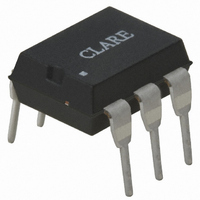
OPTOCOUPLER SGL TRANS-OUT 6-DIP
Manufacturer
Clare
Datasheet
1.LDA101STR.pdf
(5 pages)
Specifications of LDA101
Number Of Channels
1
Input Type
DC
Voltage - Isolation
3750Vrms
Current Transfer Ratio (min)
33% @ 1mA
Voltage - Output
30V
Current - Dc Forward (if)
1mA
Vce Saturation (max)
500mV
Output Type
Transistor with Base
Mounting Type
Through Hole
Package / Case
6-DIP
Relay Type
Uni-input
Lead Free Status / RoHS Status
Lead free / RoHS Compliant
Current - Output / Channel
-
Current Transfer Ratio (max)
-
Available stocks
Company
Part Number
Manufacturer
Quantity
Price

Company:
Part Number:
LDA101
Manufacturer:
IXYS
Quantity:
5 510
Part Number:
LDA101CP
Manufacturer:
N/A
Quantity:
20 000


LDA101
Absolute Maximum Ratings
Electrical Characteristics
Switching Characteristics @ 25ºC
2
Electrical absolute maximum ratings are at 25ºC
Parameters
Output Characteristics @ 25ºC (unless otherwise noted)
Phototransistor Breakdown Voltage
Phototransistor Dark Current
Saturation Voltage
Current Transfer Ratio
Output Capacitance
Input Characteristics @ 25ºC
Input Control Current
Input Voltage Drop
Common Characteristics @ 25ºC
Input to Output Capacitance
Characteristic
Turn-On Time
Turn-Off Time
Parameter
Breakdown Voltage
Reverse Input Voltage
Input Control Current
Power Dissipation
Isolation Voltage Input to Output
Operational Temperature
Storage Temperature
Pulse Width=5ms
Duty Cycle=1%
Peak (10ms)
Input
Phototransistors
1
2
Derate Linearly 1.33 mW/ºC
Derate Linearly 2.0 mW/ºC
1
2
Switching Time Test Circuit
Symbol
I
F
t
t
OFF
ON
V
CC
Test Condition
=5V, I
-40 to +125
Ratings
-40 to +85
F
=2mA, R
3750
150
150
30
50
5
1
I
C
I
=0.33mA, V
F
I
V
L
C
=1mA, V
Conditions
=1KΩ
CE
=2mA, I
25V, f=1MHz
=5V, I
I
I
C
F
Units
=10µA
=5mA
mW
V
mA
V
V
ºC
ºC
www.clare.com
-
V
A
rms
P
CE
F
F
CC
=0mA
=1mA
R
CE
=0.5V
Typ
L
=0.5V
20
7
V
CE
Units
Absolute Maximum Ratings are stress ratings. Stresses in
excess of these ratings can cause permanent damage to
the device. Functional operation of the device at conditions
beyond those indicated in the operational sections of this
data sheet is not implied.
Symbol
μs
V
BV
C
CTR
I
CE(sat)
C
CEO
V
OUT
I
I/O
CEO
F
F
V
90%
10%
I
F
CE
Min
0.9
30
33
t
-
-
-
-
-
ON
Typ
300
1.2
10
6
3
-
-
-
Max
500
0.5
1.4
1
-
-
-
-
Units
t
OFF
mA
nA
pF
pF
%
V
V
V
R04
Related parts for LDA101
Image
Part Number
Description
Manufacturer
Datasheet
Request
R

Part Number:
Description:
Clare Solar Cells
Manufacturer:
Clare, Inc.
Datasheet:
Part Number:
Description:
Clare Solar Cells
Manufacturer:
Clare, Inc.
Datasheet:
Part Number:
Description:
4 Pin SOP OptoMOS Relay
Manufacturer:
CLARE [Clare, Inc.]
Datasheet:

Part Number:
Description:
MOSFET N-CH 350V 5MA SOT-223
Manufacturer:
Clare
Datasheet:
Part Number:
Description:
MOSFET N-CH 350V 5MA SOT-223
Manufacturer:
Clare
Datasheet:

Part Number:
Description:
IC DRVR PROGRAMMABLE 16-SOIC
Manufacturer:
Clare
Datasheet:

Part Number:
Description:
IC PHONE LINE MONITOR 8-SOIC
Manufacturer:
Clare
Datasheet:

Part Number:
Description:
IC LITELINK III FULL RING 32SOIC
Manufacturer:
Clare
Datasheet:

Part Number:
Description:
LITELINK III PHONE LINE 32SOIC
Manufacturer:
Clare
Datasheet:

Part Number:
Description:
RELAY OPTO TELCOM 12OMA 8-DIP
Manufacturer:
Clare
Datasheet:
Part Number:
Description:
IC PHONE LINE MONITOR 8-SOIC
Manufacturer:
Clare
Datasheet:
Part Number:
Description:
RELAY OPTOMULTLIFUN 100MA 8FLTPK
Manufacturer:
Clare
Datasheet: