DS1921K# Maxim Integrated Products, DS1921K# Datasheet - Page 19
DS1921K#
Manufacturer Part Number
DS1921K#
Description
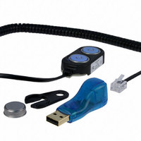
KIT IBUTTON THERMOCHRON
Manufacturer
Maxim Integrated Products
Series
iButton®r
Specifications of DS1921K#
Lead Free Status / RoHS Status
Lead free / RoHS Compliant
Memory Size
-
Memory Type
-
Lead Free Status / Rohs Status
Lead free / RoHS Compliant
Available stocks
Company
Part Number
Manufacturer
Quantity
Price


Next, the low temperature and high temperature thresh-
olds that specify the temperature tolerance band must
be defined. The Temperature Conversion section
describes how to convert a temperature value into the
binary code to be written to the threshold registers.
The state of the search condition bits in the Control
register does not affect the mission. If multiple devices
are connected to form a 1-Wire net, the setting of the
search condition enables these devices to participate
in the conditional search if certain events, such as
timer or temperature alarms, have occurred. Details
on the search conditions are found in the ROM
Function Commands section and in the Control regis-
ter description.
The setting of the rollover-enable bit (RO) and sample
rate depends on the duration of the mission and the
monitoring requirements. If the most recent temperature
history is important, the rollover should be enabled
(RO = 1). Otherwise, one should estimate the duration
of the mission in minutes and divide the number by
2048 to calculate the value of the sample rate (number
of minutes between temperature conversions). For
example, if the estimated duration of a mission is 10
days (14,400min), then the 2048-byte capacity of the
data-log memory would be sufficient to store a new
value every 7min. If the DS1921G’s data-log memory is
not large enough to store all temperature readings, one
can use several devices and set the Mission Start Delay
to values that make the second device start recording
as soon as the memory of the first device is full and so
on. The RO bit needs to be set to 0 to disable rollover
that would otherwise overwrite the recorded tempera-
ture log.
After the RO bit and the Mission Start Delay are set, the
Sample Rate register is the last element of data that is
written. The sample rate can be any value from 1 to
255, coded as an unsigned 8-bit binary number. As
soon as the sample rate is written, the DS1921G sets
the MIP flag and clears the MEMCLR flag. After as
many minutes as specified by the Mission Start Delay
are over, the device waits for the next minute boundary,
then wakes up, copies the current time and date to the
Mission Timestamp register, and makes the first tem-
perature conversion of the mission. This increments
both the Mission Samples Counter and Device Samples
Counter. All subsequent temperature measurements
are taken on minute boundaries specified by the value
in the Sample Rate register. One can read the memory
of the DS1921G to watch the mission as it progresses.
Care should be taken to avoid memory access con-
flicts. See the Memory Access Conflicts section for
details.
______________________________________________________________________________________
Because of the serial data transfer, the DS1921G
employs three address registers, called TA1, TA2, and
E/S (Figure 9). Registers TA1 and TA2 must be loaded
with the target address to which the data is written or
from which data is sent to the master upon a read com-
mand. Register E/S acts like a byte counter and transfer
status register. It is used to verify data integrity with
write commands. Therefore, the master has only read
access to this register. The lower 5 bits of the E/S regis-
ter indicate the address of the last byte that has been
written to the scratchpad. This address is called Ending
Offset. Bit 5 of the E/S register, called PF or partial byte
flag, is set if the number of data bits sent by the master
is not an integer multiple of 8. Bit 6 is always a 0. Note
that the lowest 5 bits of the target address also deter-
mine the address within the scratchpad where interme-
diate storage of data begins. This address is called
byte offset. If the target address for a write command is
13Ch, for example, then the scratchpad stores incom-
ing data beginning at the byte offset 1Ch and is full
after only 4 bytes. The corresponding ending offset in
this example is 1Fh. For the best economy of speed
and efficiency, the target address for writing should
point to the beginning of a new page, i.e., the byte off-
set is 0. Thus, the full 32-byte capacity of the scratch-
pad is available, resulting also in the ending offset of
1Fh. However, it is possible to write one or several con-
tiguous bytes somewhere within a page. The ending
offset together with the partial and overflow flag are a
means to support the master checking the data integri-
ty after a write command. The highest valued bit of the
E/S register, called authorization accepted (AA), indi-
cates that a valid copy command for the scratchpad
has been received and executed. Writing data to the
scratchpad clears this flag.
To write data to the DS1921G, the scratchpad must be
used as intermediate storage. First, the master issues
the Write Scratchpad command to specify the desired
target address, followed by the data to be written to the
scratchpad. In the next step, the master sends the
Read Scratchpad command to read the scratchpad
and to verify data integrity. As preamble to the scratch-
pad data, the DS1921G sends the requested target
address TA1 and TA2 and the contents of the E/S regis-
ter. If the PF flag is set, data did not arrive correctly in
the scratchpad. The master does not need to continue
reading; it can start a new trial to write data to the
scratchpad. Similarly, a set AA flag indicates that the
Thermochron iButton
Writing with Verification
Address Registers and
Transfer Status
19
Related parts for DS1921K#
Image
Part Number
Description
Manufacturer
Datasheet
Request
R

Part Number:
Description:
MAX7528KCWPMaxim Integrated Products [CMOS Dual 8-Bit Buffered Multiplying DACs]
Manufacturer:
Maxim Integrated Products
Datasheet:
Part Number:
Description:
Single +5V, fully integrated, 1.25Gbps laser diode driver.
Manufacturer:
Maxim Integrated Products
Datasheet:
Part Number:
Description:
Single +5V, fully integrated, 155Mbps laser diode driver.
Manufacturer:
Maxim Integrated Products
Datasheet:
Part Number:
Description:
VRD11/VRD10, K8 Rev F 2/3/4-Phase PWM Controllers with Integrated Dual MOSFET Drivers
Manufacturer:
Maxim Integrated Products
Datasheet:
Part Number:
Description:
Highly Integrated Level 2 SMBus Battery Chargers
Manufacturer:
Maxim Integrated Products
Datasheet:
Part Number:
Description:
Current Monitor and Accumulator with Integrated Sense Resistor; ; Temperature Range: -40°C to +85°C
Manufacturer:
Maxim Integrated Products
Part Number:
Description:
TSSOP 14/A�/RS-485 Transceivers with Integrated 100O/120O Termination Resis
Manufacturer:
Maxim Integrated Products
Part Number:
Description:
TSSOP 14/A�/RS-485 Transceivers with Integrated 100O/120O Termination Resis
Manufacturer:
Maxim Integrated Products
Part Number:
Description:
QFN 16/A�/AC-DC and DC-DC Peak-Current-Mode Converters with Integrated Step
Manufacturer:
Maxim Integrated Products
Part Number:
Description:
TDFN/A/65V, 1A, 600KHZ, SYNCHRONOUS STEP-DOWN REGULATOR WITH INTEGRATED SWI
Manufacturer:
Maxim Integrated Products
Part Number:
Description:
Integrated Temperature Controller f
Manufacturer:
Maxim Integrated Products
Part Number:
Description:
SOT23-6/I�/45MHz to 650MHz, Integrated IF VCOs with Differential Output
Manufacturer:
Maxim Integrated Products
Part Number:
Description:
SOT23-6/I�/45MHz to 650MHz, Integrated IF VCOs with Differential Output
Manufacturer:
Maxim Integrated Products
Part Number:
Description:
EVALUATION KIT/2.4GHZ TO 2.5GHZ 802.11G/B RF TRANSCEIVER WITH INTEGRATED PA
Manufacturer:
Maxim Integrated Products
Part Number:
Description:
QFN/E/DUAL PCIE/SATA HIGH SPEED SWITCH WITH INTEGRATED BIAS RESISTOR
Manufacturer:
Maxim Integrated Products
Datasheet: