SDCFCF-002G-388 SanDisk, SDCFCF-002G-388 Datasheet - Page 22
SDCFCF-002G-388
Manufacturer Part Number
SDCFCF-002G-388
Description
COMPACT FLASH IND 2GB FIXED
Manufacturer
SanDisk
Type
CompactFlashr
Datasheet
1.SDCFCF-001G-388.pdf
(97 pages)
Specifications of SDCFCF-002G-388
Memory Size
2GB
Memory Type
CompactFLASH
Density
2GByte
Operating Supply Voltage (typ)
3.3/5V
Operating Temperature (min)
0C
Operating Temperature (max)
70C
Package Type
Not Required
Mounting
Desktop
Pin Count
50
Operating Temperature Classification
Commercial
Operating Supply Voltage (min)
3.135/4.5V
Operating Supply Voltage (max)
3.465/5.5V
Programmable
Yes
Lead Free Status / RoHS Status
Lead free / RoHS Compliant


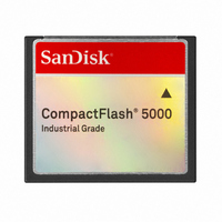
SanDisk Industrial Grade CompactFlash 5000
(True IDE Mode)
-INPACK (PC Card Memory
Mode) -INPACK (PC Card I/O
Mode) -DMARQ (True IDE
Mode)
-IORD (PC Card Memory
Mode) -IORD (PC Card I/O
Mode) (True IDE Mode)
-IOWR (PC Card Memory
Mode)
-IOWR (PC Card I/O Mode)
(True IDE Mode)
-OE (PC Card Memory Mode)
-OE (PC Card I/O Mode) -ATA
SEL (True IDE Mode)
RDY/-BSY (PC Card Memory
Mode) -IREQ (PC Card I/O
Mode) INTRQ (True IDE
Mode)
-REG (PC Card Memory
Mode) -REG (PC Card I/O
Mode)
© 2007 SanDisk® Corporation
O
I
I
I
O
I
43
34
35
37
44
9
This signal is not used in this mode. The card asserts the Input Acknowledge signal when it is selected and
responding to an I/O read cycle at the address that is on the address bus. The host uses this signal to control
the enable of any input data buffers between the card and the CPU. This signal is used for DMA data transfers
between host and device and is asserted by the device when it is ready to transfer data to or from the host. The
direction of data transfer is controlled by DIOR- and DIOW-. This signal is used in a handshake manner with
DMACK- (i.e., the device waits until the host asserts DMACK- before negating DMARQ, and reasserting
DMARQ if there is more data to transfer).
This signal is not used in this mode. This is an I/O read strobe generated by the host. This signal gates I/O data
onto the bus from the card when the card is configured to use the I/O interface.
This signal is not used in this mode.
The I/O write strobe pulse is used to clock I/O data on the Card Data bus into the card controller registers when
the card is configured to use the I/O interface. The clocking will occur on the negative to positive edge of the
signal (trailing edge).
This is an output enable strobe generated by the host interface. It is used to read data from the card in Memory
Mode and to read the CIS and configuration registers. In PC Card I/O Mode, this signal is used to read the CIS
and configuration registers. To enable True IDE Mode this input should be grounded by the host.
In Memory Mode, this signal is set high when the card is ready to accept a new data transfer operation and
held low when the card is busy. The host memory card socket must provide a pull-up resistor. At power up and
at reset the RDY/-BSY signal is held low (busy) until the card has completed its power up or reset function. No
access of any type should be made to the card during this time. The RDY/-BSY signal is held high (disabled
from being busy) whenever the following condition is true: the card has been powered up with +RESET
continuously disconnected or asserted. I/O Operation–After the card has been configured for I/O operation, this
signal is used as an interrupt request. This line is strobed low to generate a pulse mode interrupt or held low for
a level mode interrupt. In True IDE Mode, this signal is the active high Interrupt Request to the host.
This Attribute Memory Select signal is used during memory cycles to distinguish between Common Memory
and Register (Attribute) Memory accesses: High for common memory and low for attribute memory. The signal
must also be active (low) during I/O cycles when the I/O address is on the bus.
15
Product Manual
March 2007
Related parts for SDCFCF-002G-388
Image
Part Number
Description
Manufacturer
Datasheet
Request
R

Part Number:
Description:
COMPACT FLASH IND 1GB FIXED
Manufacturer:
SanDisk
Datasheet:
Part Number:
Description:
COMPACT FLASH IND 512MB FIXED
Manufacturer:
SanDisk
Datasheet:
Part Number:
Description:
COMPACT FLASH IND 4GB FIXED
Manufacturer:
SanDisk
Datasheet:
Part Number:
Description:
COMPACT FLASH IND 8GB FIXED
Manufacturer:
SanDisk
Datasheet:

Part Number:
Description:
IC MDOC G4 2GB 69-FBGA
Manufacturer:
SanDisk
Datasheet:
Part Number:
Description:
IC MDOC P3 256MB 48-TSOP
Manufacturer:
SanDisk
Datasheet:
Part Number:
Description:
IC MDOC P3 256MB 48-TSOP
Manufacturer:
SanDisk
Datasheet:
Part Number:
Description:
IC MDOC P3 256MB 48-TSOP
Manufacturer:
SanDisk
Datasheet:
Part Number:
Description:
IC MDOC H1 8GB 115-FBGA
Manufacturer:
SanDisk
Datasheet:
Part Number:
Description:
IC MDOC H3 1GB FBGA
Manufacturer:
SanDisk
Datasheet: