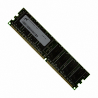
MT8VDDT6464AY-40BF4 Micron Technology Inc, MT8VDDT6464AY-40BF4 Datasheet - Page 15

MT8VDDT6464AY-40BF4
Manufacturer Part Number
MT8VDDT6464AY-40BF4
Description
MODULE DDR SDRAM 512MB 184-DIMM
Manufacturer
Micron Technology Inc
Datasheet
1.MT8VDDT6464AY-40BF4.pdf
(26 pages)
Specifications of MT8VDDT6464AY-40BF4
Memory Type
DDR SDRAM
Memory Size
512MB
Speed
400MT/s
Package / Case
184-DIMM
Lead Free Status / RoHS Status
Lead free / RoHS Compliant
Other names
557-1232
MT8VDDT6464AY-40BF4
MT8VDDT6464AY-40BF4
Table 11:
AC Operating Specifications
Table 12:
PDF: 09005aef80a43556, Source: 09005aef80a43534
DDA8C16_32_64x64AG_2.fm - Rev. E 4/06 EN
Operating current: One device bank; Active-Precharge;
t
and control inputs changing once every two clock cycles
Operating current: One device bank; Active-Read-Pre-charge; Burst = 2;
t
changing once per clock cycle
PRECHARGE power-down standby current: All device banks idle; Power-down
mode;
Idle standby current: CS# = HIGH; All device banks idle;
HIGH; Address and other control inputs changing once per clock cycle. V
for DQ, DQS, and DM
ACTIVE power-down standby current: One device bank active; Power-down
mode;
ACTIVE standby current: CS# = HIGH; CKE = HIGH; One device bank; Active-
Precharge;
changing twice per clock cycle; Address and other control inputs changing once
per clock cycle
Operating current: Burst = 2; Reads; Continuous burst; One device bank active;
Address and control inputs changing once per clock cycle;
0mA
Operating current: Burst = 2; Writes; Continuous burst; One device bank active;
Address and control inputs changing once per clock cycle;
DM, and DQS inputs changing twice per clock cycle
AUTO REFRESH current
SELF REFRESH current: CKE ≤ 0.2V
Operating current: Four device bank interleaving READs (BL= 4) with auto
precharge,
change only during ACTIVE, READ, or WRITE commands
CK =
RC =
t
t
CK (MIN); DQ, DM, and DQS inputs changing once per clock cycle; Address
RC (MIN);
t
t
CK =
CK =
t
t
RC = MIN
RC =
t
t
CK (MIN); CKE = LOW
CK (MIN); CKE = LOW
I
DDR SDRAM components only
Notes: 1–5, 8, 10, 12, 30; notes appear on pages 16–18; 0°C ≤ T
Module and Component Speed Grade Table
DD
t
t
CK =
RAS (MAX);
Specifications and Conditions – 512MB
t
RC allowed;
t
CK (MIN); I
Recommended AC operating conditions are given in the DDR component data sheets.
Component specifications are available on Micron’s Web site:
ucts/ddrsdram.
in the following table:
Parameter/Condition
t
CK =
OUT
t
CK =
t
CK (MIN); DQ, DM, and DQS inputs
128MB, 256MB, 512MB (x64, SR): PC3200 184-Pin DDR UDIMM
= 0mA; Address and control inputs
t
Module Speed Grade
CK (MIN); Address and control inputs
Module speed grades correlate with component speed grades as shown
-40B
t
t
RC =
CK =
t
CK =
t
CK =
15
t
t
t
t
REFC =
REFC = 7.8125µs
RC (MIN);
CK (MIN); CKE =
t
CK (MIN); I
t
CK (MIN); DQ,
t
RFC (MIN)
Micron Technology, Inc., reserves the right to change products or specifications without notice.
IN
= V
OUT
A
REF
≤ +70°C; V
=
Symbol
I
I
I
I
I
I
I
DD 4 W
I
I
DD 3 N
I
DD 5 A
I
I
DD 2 P
DD 2 F
DD 3 P
DD 4 R
DD 0
DD 1
DD 5
DD 6
DD 7
Component Speed Grade
DD
Electrical Specifications
= V
DD
www.micron.com/prod-
1,240
1,480
1,520
1,560
2,760
3,600
Max
-40B
©2005 Micron Technology, Inc. All rights reserved.
440
360
440
40
88
40
Q = +2.6V ±0.1V
-5
Units
mA
mA
mA
mA
mA
mA
mA
mA
mA
mA
mA
mA
15, 18, 27
15, 18, 27
Notes
14, 25
14, 25
14, 25
14, 27
16, 27
14, 26
18
24
14
9


