MT8VDDT6464HDY-40BF2 Micron Technology Inc, MT8VDDT6464HDY-40BF2 Datasheet
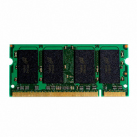
MT8VDDT6464HDY-40BF2
Specifications of MT8VDDT6464HDY-40BF2


Related parts for MT8VDDT6464HDY-40BF2


MT8VDDT6464HDY-40BF2 Summary of contents
Page 1
... RCD and RP for -335 modules show 18ns to align with industry specifications; Micron Technology, Inc., reserves the right to change products or specifications without notice. 1 Features 200-Pin SODIMM (MO-224) Marking 2 ≤ +70°C) None A ≤ +85°C) ...
Page 2
... Data sheets for the base devices can be found on Micron’s Web site. 2. All part numbers end with a two-place code (not shown) that designates component and PCB revisions. Consult factory for current revision codes. Example: MT8VDDT6464HDY-335F2. PDF: 09005aef80765fab/Source: 09005aef806e1d28 DD8C32_64x64HD.fm - Rev. E 11/08 EN ...
Page 3
Pin Assignments and Descriptions Table 5: Pin Assignments 200-Pin SODIMM Front Pin Symbol Pin Symbol Pin Symbol Pin Symbol 101 REF DQ19 103 SS 5 DQ0 55 DQ24 105 7 DQ1 57 ...
Page 4
Table 6: Pin Descriptions Symbol A0–A12 BA0, BA1 CK0, CK0#, CK1, CK1# CKE0, CKE1 DM0–DM7 RAS#, CAS#, WE# S0#, S1# SA0–SA2 SCL DQ0–DQ63 DQS0–DQS7 SDA DDSPD V REF PDF: 09005aef80765fab/Source: 09005aef806e1d28 DD8C32_64x64HD.fm - Rev. ...
Page 5
Functional Block Diagram Figure 2: Functional Block Diagram S1# S0# CS# DQS0 UDQS DM0 UDM DQ0 DQ DQ1 DQ DQ2 DQ DQ3 DQ DQ4 DQ DQ5 DQ U1 DQ6 DQ DQ7 DQ DQS1 LDQS DM1 LDM DQ8 DQ DQ9 DQ ...
Page 6
... READs and by the memory controller during WRITEs. DQS is edge-aligned with data for READs and center-aligned with data for WRITEs. DDR SDRAM modules operate from differential clock inputs (CK and CK#); the crossing of CK going HIGH and CK# going LOW will be referred to as the positive edge of CK. ...
Page 7
Electrical Specifications Stresses greater than those listed in Table 7 may cause permanent damage to the module. This is a stress rating only, and functional operation of the module at these or any other conditions outside those indicated on the ...
Page 8
... Design Considerations Simulations Micron memory modules are designed to optimize signal integrity through carefully designed terminations, controlled board impedances, routing topologies, trace length matching, and decoupling. However, good signal integrity starts at the system level. Micron encourages designers to simulate the signal characteristics of the system’s memory bus to ensure adequate signal integrity of the entire memory system ...
Page 9
I Specifications DD Table 9: I Specifications and Conditions – 256MB (Die Revision K) DD Values are for the MT46V16M16 DDR SDRAM only and are computed from values specified in the 256Mb (16 Meg x 16) component data sheet Parameter/Condition ...
Page 10
Table 10: I Specifications and Conditions – 256MB (All other Die Revisons) DD Values are for the MT46V16M16 DDR SDRAM only and are computed from values specified in the 256Mb (16 Meg x 16) component data sheet Parameter/Condition Operating one ...
Page 11
Table 11: I Specifications and Conditions – 512MB DD Values are for the MT46V32M16 DDR SDRAM only and are computed from values specified in the 256Mb (32 Meg x 16) component data sheet Parameter/Condition Operating one device bank active-precharge current: ...
Page 12
Serial Presence-Detect Table 12: Serial Presence-Detect EEPROM DC Operating Conditions Parameter/Condition Supply voltage Input high voltage: Logic 1; All inputs Input low voltage: Logic 0; All inputs Output low voltage 3mA OUT Input leakage current GND ...
Page 13
Module Dimensions Figure 3: 200-Pin DDR SODIMM 2.0 (0.079) R (2X) U1 1.8 (0.071) (2X) 6.0 (0.236) TYP 1.0 (0.39) 2.0 (0.079) TYP U8 Pin 200 Notes: 1. All dimensions are in millimeters (inches); MAX/MIN or typical (TYP) where noted. ...