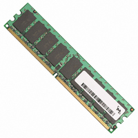
MT36HTJ51272Y-40EA2 Micron Technology Inc, MT36HTJ51272Y-40EA2 Datasheet - Page 8

MT36HTJ51272Y-40EA2
Manufacturer Part Number
MT36HTJ51272Y-40EA2
Description
MODULE DDR2 4GB 240-DIMM
Manufacturer
Micron Technology Inc
Datasheet
1.MT36HTJ51272Y-40EA2.pdf
(14 pages)
Specifications of MT36HTJ51272Y-40EA2
Memory Type
DDR2 SDRAM
Memory Size
4GB
Speed
400MT/s
Package / Case
240-DIMM
Lead Free Status / RoHS Status
Lead free / RoHS Compliant
AC Timing and Operating Conditions
Table 8:
Register and PLL Specifications
Table 9:
PDF: 09005aef822553c2/Source: 09005aef822553af
HT36HTJ51272.fm - Rev. B 7/06 EN
Parameter
DC high-level
input voltage
DC low-level
input voltage
AC high-level
input voltage
AC low-level
input voltage
Output high voltage
Output low voltage
Input current
Static standby
Static operating
Dynamic operating –
clock tree
Dynamic operating
(per each input)
Input capacitance
(per device, per pin)
Module and Component Speed Grade Table
Register (SSTU32868 devices or equivalent JESD82-16)
Module Speed Grade
Notes:
Symbol
V
V
V
V
I
I
IH
IH
IL
IL
V
V
DDD
DDD
I
I
DD
DD
C
OH
(
(
I
(
(
OL
I
DC
AC
Recommended AC operating conditions are given in the DDR2 component data sheets.
Component specifications are available on Micron’s Web site: www.micron.com. Module
speed grades correlate with component speed grades as shown in Table 8:
-667
-53E
-40E
1. Specifications for the register listed above are critical for proper operation of DDR2 SDRAM
DC
AC
I
)
)
)
)
registered DIMMs. These are meant to be a subset of the parameters for the specific device
used on the module. Detailed information for this register is available in JEDEC Standard
JESD82.
Address, control,
Address, control,
Address, control,
Address, control,
All inputs except
Parity output
Parity output
command
command
command
command
All pins
All pins
All pins
RESET#
RESET#
Pins
n/a
n/a
RESET# = V
RESET# = V
One data input switching at
V
V
switching 50% duty cycle;
switching 50% duty cycle
4GB (x72, ECC, DR) 240-Pin DDR2 SDRAM RDIMM
IL
IL
RESET# = V
t
V
(
(
CK/2, 50% duty cycle
AC
AC
V
I
V
V
= V
I
I
RESET# = V
I
), I0 = 0; CK and CK#
), I0 = 0; CK and CK#
= V
= V
= V
8
V
Condition
IH
DD
LVCMOS
LVCMOS
SSTL_18
SSTL_18
SSTL_18
SSTL_18
DD
DD
DD
I/O = 0
REF
DD
(
AC
Q = 1.8V
, V
, V
Q or V
Q or V
SS
) or V
±250mV;
Q (I/O = 0)
I
I
= V
= V
Micron Technology, Inc., reserves the right to change products or specifications without notice.
SS
AC Timing and Operating Conditions
Q;
IL
SS
IH
IH
SS
(
Q
(
(
Q
DC
AC
AC
)
) or
) or
Component Speed Grade
V
V
REF
REF
(
(
Min
DC
DC
1.2
2.5
–5
0
0
–
–
–
–
–
–
-37E
) + 250
-5E
) +125
-3
©2003 Micron Technology, Inc. All rights reserved.
manufacturer
manufacturer
manufacturer
V
V
V
REF
REF
Varies by
Varies by
Varies by
DD
40mA
(
(
Max
Q + 250
V
DC
DC
100
0.5
3.5
5
DD
–
) - 125
) - 250
Units
mV
mV
mV
mV
mV
mV
µA
µA
µA
µA
µA
pF
pF


