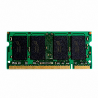
MT16HTS25664HY-667A1 Micron Technology Inc, MT16HTS25664HY-667A1 Datasheet - Page 9

MT16HTS25664HY-667A1
Manufacturer Part Number
MT16HTS25664HY-667A1
Description
MODULE DDR2 2GB 200SODIMM
Manufacturer
Micron Technology Inc
Specifications of MT16HTS25664HY-667A1
Memory Type
DDR2 SDRAM
Memory Size
2GB
Speed
667MT/s
Package / Case
200-SODIMM
Main Category
DRAM Module
Sub-category
DDR2 SDRAM
Module Type
200SODIMM
Device Core Size
64b
Organization
256Mx64
Total Density
2GByte
Chip Density
1Gb
Maximum Clock Rate
667MHz
Operating Supply Voltage (typ)
1.8V
Operating Current
1.176A
Number Of Elements
16
Operating Supply Voltage (max)
1.9V
Operating Supply Voltage (min)
1.7V
Operating Temp Range
0C to 70C
Operating Temperature Classification
Commercial
Pin Count
200
Mounting
Socket
Lead Free Status / RoHS Status
Lead free / RoHS Compliant
Table 7:
PDF: 09005aef821e5bf3/Source: 09005aef82198d54
HTS16C256x64H.fm - Rev. A 4/06 EN
Parameter/Condition
Operating one bank active-precharge current;
(I
commands; Address bus inputs are SWITCHING; Data bus inputs are
SWITCHING.
Operating one bank active-read-precharge current; I
CL = CL(I
t
bus inputs are SWITCHING; Data pattern is same as I
Precharge power-down current; All device banks idle;
is LOW; Other control and address bus inputs are STABLE; Data bus inputs are
FLOATING.
Precharge quiet standby current; All device banks idle;
CKE is HIGH, S# is HIGH; Other control and address bus inputs are STABLE;
Data bus inputs are FLOATING.
Precharge standby current; All device banks idle;
HIGH, S# is HIGH; Other control and address bus inputs are SWITCHING; Data
bus inputs are SWITCHING.
Active power-down current; All device banks open;
t
are STABLE; Data bus inputs are FLOATING.
Active standby current; All device banks open;
MAX (I
Other control and address bus inputs are SWITCHING; Data bus inputs are
SWITCHING.
Operating burst write current; All device banks open, Continuous burst
writes; BL = 4, CL = CL (I
=
inputs are SWITCHING; Data bus inputs are SWITCHING.
Operating burst read current; All device banks open, Continuous burst
reads, I
MAX (I
Address bus inputs are SWITCHING; Data bus inputs are SWITCHING.
Burst refresh current;
interval; CKE is HIGH, S# is HIGH between valid commands; Other control and
address bus inputs are SWITCHING; Data bus inputs are SWITCHING.
Self refresh current; CK and CK# at 0V; CKE ≤ 0.2V; Other control and
address bus inputs are FLOATING; Data bus inputs are FLOATING.
Operating bank interleave read current; All device banks interleaving
reads, I
(I
HIGH between valid commands; Address bus inputs are STABLE during
DESELECTs; Data bus inputs are SWITCHING; See I
Note:
a. Value calculated as one module rank in this operating condition, and all other module ranks in I
b. Value calculated reflects all module ranks in this operating condition.
RCD =
CK (I
DD
DD
t
RP (I
),
),
DD
t
t
RAS =
RC =
DD
DD
DD
OUT
t
OUT
); CKE is LOW; Other control and address bus inputs
RCD (I
DD
),
); CKE is HIGH, S# is HIGH between valid commands; Address bus
),
= 0mA; BL = 4, CL = CL (I
), AL = 0;
t
= 0mA; BL = 4, CL = CL (I
t
t
RP =
RP =
RC(I
t
RAS MIN (I
DDR2 I
Values shown for DDR2 SDRAM components only
DD
DD
); CKE is HIGH, S# is HIGH between valid commands; Address
t
t
RP(I
RP (I
),
t
t
CK =
RRD =
DD
DD
DD
DD
); CKE is HIGH, S# is HIGH between valid commands;
DD
t
); CKE is HIGH, S# is HIGH between valid commands;
CK =
Specifications and Conditions – 2GB
), AL = 0;
t
); CKE is HIGH, S# is HIGH between valid
CK (I
t
RRD(I
t
CK (I
DD
DD
),
DD
t
CK =
DD
DD
t
),
RC =
), AL =
); Refresh command at every
), AL = 0;
t
RCD =
t
CK (I
t
RC (I
t
RCD (I
t
DD
RCD(I
DD
t
CK =
),
DD
),
t
t
DD
CK =
RAS =
t
t
7 Conditions for detail.
DD
DD
CK =
RAS =
t
)-1 ×
CK =
t
CK (I
4W.
); CKE is HIGH, S# is
t
CK =
t
CK(I
t
t
t
RAS MAX (I
OUT
CK =
t
CK (I
t
CK (I
2GB: (x64, DR) 200-Pin DDR2 SDRAM SODIMM
t
DD
t
CK (I
RAS MIN (I
CK =
DD
9
),
= 0mA; BL = 4,
DD
),
t
Fast PDN Exit
MR[12] = 0
Slow PDN Exit
MR[12] = 1
t
DD
DD
CK (I
RAS =
t
t
),
CK (I
RAS =
);
); CKE is
t
t
t
RFC (I
RC =
CK =
DD
DD
Micron Technology, Inc., reserves the right to change products or specifications without notice.
DD
DD
t
); CKE
RAS
),
t
),
);
RAS
t
t
t
DD
RC
CK
RP
)
Symbol
I
I
I
I
I
I
I
DD
DD
DD
DD
I
I
DD
DD
DD
I
I
I
DD
DD
DD
DD
DD
4W
2Q
2N
3N
4R
2P
3P
0
1
5
6
7
b
b
a
a
a
b
b
b
b
b
a
a
Electrical Specifications
1,200
1,040
1,120
1,480
1,680
4,320
2,760
-667
840
112
960
640
112
80
©2006 Micron Technology, Inc. All rights reserved.
DD
1,080
1,200
4,000
2,400
-53E
680
800
656
720
480
800
80
80
80
2
P
(CKE LOW) mode.
1,000
1,120
3,840
2,400
-40E
680
800
560
560
400
640
80
80
80
Units
mA
mA
mA
mA
mA
mA
mA
mA
mA
mA
mA
mA
mA


