LQ038Q7DB03R Sharp Microelectronics, LQ038Q7DB03R Datasheet - Page 9
LQ038Q7DB03R
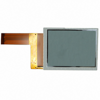
Manufacturer Part Number
LQ038Q7DB03R
Description
LCD TFT 3.8" 240X320 QVGA
Manufacturer
Sharp Microelectronics
Datasheet
1.LQ038Q7DB03R.pdf
(24 pages)
Specifications of LQ038Q7DB03R
Display Type
LCD - Color
Display Mode
*
Viewing Area
76.80mm L x 57.60mm W
Dot Pitch
0.24mm x 0.24mm
Dot Pixels
320 x 240 (QVGA)
Pixel Density
240 x 320
Module Size (w X H X T)
69 mm x 88.6 mm x 3.4 mm
Backlighting
White
Diagonal
3.8 in
Maximum Operating Temperature
+ 70 C
Minimum Operating Temperature
- 25 C
Operating Temperature Range
- 25 C to + 70 C
Product
Displays
Touch Panel
No Touch Panel
Viewing Area (w X H)
57.6 mmx 76.8 mm
Lead Free Status / RoHS Status
Lead free / RoHS Compliant
Interface
-
Backlight
-
Dot Size
-
Lead Free Status / Rohs Status
Lead free / RoHS Compliant
Other names
425-2649
Available stocks
Company
Part Number
Manufacturer
Quantity
Price
Company:

Part Number:
LQ038Q7DB03R
Manufacturer:
Sharp Microelectronics
Quantity:
135
Company:
Part Number:
LQ038Q7DB03R
Manufacturer:
SHARP
Quantity:
1 000


※ Cautions when you turn on or off the power supply
【Note 7-1】These are standard input voltages for gray scale. When V
【Note 7-2】It must be kept that 3.0V≦(V
【Note 7-3】The same phase and amplitude with V
【Note 7-4】DCLK,SPL,SPR,LBR,LP,PS,R0∼R5,G0∼G5 and B0∼B5 terminals are applied.
【Note 7-5】DCLK,SPL,SPR,LBR,LP,R0∼R5,G0∼G5 and B0∼B5 terminals are applied.
【Note 7-6】PS terminal is applied.
【Note 7-7】MOD,CLS,SPS and U/L terminals are applied.
【Note 7-8】V
B)
【Note 7-9】Calculated reference value(I
LED voltage
LED current
Power consumption
Table 7
① Turn on or off the power supply with simultaneously or the following sequence.
② The input signal of “MOD” Terminals(Pin No.51 and No.52) must be low voltage when turning on
Back light driving section
the power supply, and it is held until more than double vertical periods after V
completely. After then, it must be held high voltage until turning off the power supply.(Connect
Pin No.51 and No.52 terminals to the same signal.)
Parameter
voltage should be alternated polarity. V0(black) is different polarity alternating signal of
V
standard input voltage shift positive way for LCD characteristics (V0→V1→V2→V3→V4).
This sift amount is adjusted so as to no flicker of each standard
input voltage after
DC bias voltage of V
V
module .
COMAC
COM
COMDC
Turn on … V
Turn off … V
. V4(white) is the same polarity alternating signal of V
should be alternated on V
bias is adjusted so as to minimize flicker or maximum contrast every each
SHD
DD
Symbol
W
→V
→ V
V
COM
I
L
L
L
SHA
EE
and V0 is adjusted.
→ V
→ V
CC
MIN
L
−
−
−
×V
-V
CC
SS
SS
COMDC
L
)
→ V
→ V
)≦3.6V.
COM
CC
SS
every 1 horizontal period and 1 vertical period.
. V
TYP
32.4
486
15
→V
→ V
EEDC
SHA
EE
is center of V
→ V
→ V
MAX
36.0
720
20
SHD
COM
DD
COM
is alternated polarity, these
EE
. Center voltage of each
Units
mW
mA
.
V
Remarks terminal
【Note 7-9】
CC
LCP-05007−6
is turned on
Ta=25℃
Related parts for LQ038Q7DB03R
Image
Part Number
Description
Manufacturer
Datasheet
Request
R

Part Number:
Description:
IC FLASH 32MBIT 110NS 56SSOP
Manufacturer:
Sharp Microelectronics
Datasheet:

Part Number:
Description:
IC FLASH 16MBIT 100NS 56TSOP
Manufacturer:
Sharp Microelectronics
Datasheet:

Part Number:
Description:
IC FLASH 64MBIT 120NS 56TSOP
Manufacturer:
Sharp Microelectronics
Datasheet:

Part Number:
Description:
IC FLASH 16MBIT 90NS 48TSOP
Manufacturer:
Sharp Microelectronics
Datasheet:
Part Number:
Description:
IC SRAM 16KBIT 100NS 24DIP
Manufacturer:
Sharp Microelectronics
Datasheet:
Part Number:
Description:
IC SRAM 16KBIT 100NS 24SOP
Manufacturer:
Sharp Microelectronics
Datasheet:
Part Number:
Description:
IC SRAM 64KBIT 100NS 28DIP
Manufacturer:
Sharp Microelectronics
Datasheet:
Part Number:
Description:
IC SRAM 64KBIT 100NS 28SOP
Manufacturer:
Sharp Microelectronics
Datasheet:
Part Number:
Description:
IC SRAM 64KBIT 100NS 28SOP
Manufacturer:
Sharp Microelectronics
Datasheet:
Part Number:
Description:
IC SRAM 256KBIT 70NS 28DIP
Manufacturer:
Sharp Microelectronics
Datasheet:
Part Number:
Description:
IC FLASH 8MBIT 90NS 48TSOP
Manufacturer:
Sharp Microelectronics
Datasheet:
Part Number:
Description:
IC FLASH 8MBIT 85NS 40TSOP
Manufacturer:
Sharp Microelectronics
Datasheet:
Part Number:
Description:
IC FLASH 8MBIT 85NS 40TSOP
Manufacturer:
Sharp Microelectronics
Datasheet:
Part Number:
Description:
IC FLASH 16MBIT 90NS 48TSOP
Manufacturer:
Sharp Microelectronics
Datasheet:
Part Number:
Description:
IC FLASH 16MBIT 70NS 56TSOP
Manufacturer:
Sharp Microelectronics
Datasheet: