HDSP-2112 Avago Technologies US Inc., HDSP-2112 Datasheet - Page 9
HDSP-2112
Manufacturer Part Number
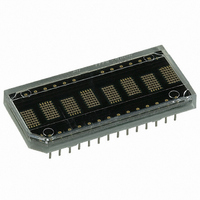
HDSP-2112
Description
LED DISPLAY 5X7 8CHAR 5MM HE RED
Manufacturer
Avago Technologies US Inc.
Series
HDSP-211xr
Specifications of HDSP-2112
Display Type
Alphanumeric
Package / Case
28-DIP
Color
Red
Size / Dimension
1.68" L x 0.77" W x 0.21" H (42.59mm x 19.58mm x 5.31mm)
Number Of Digits/alpha
8
Common Pin
*
Digit/alpha Size
0.20" (5mm)
Number Of Digits
8
Character Size
5 mm x 7 mm
Illumination Color
Red
Wavelength
635 nm
Operating Voltage
4.5 V to 5.5 V
Maximum Operating Temperature
+ 85 C
Minimum Operating Temperature
- 45 C
Luminous Intensity
7.5 mcd
Character Height
5⁄7 mm
Lead Free Status / RoHS Status
Lead free / RoHS Compliant
Lead Free Status / RoHS Status
Lead free / RoHS Compliant, Lead free / RoHS Compliant
Other names
516-1161-5
Available stocks
Company
Part Number
Manufacturer
Quantity
Price
Company:

Part Number:
HDSP-2112
Manufacturer:
FAIRCHILD
Quantity:
2 000
Part Number:
HDSP-2112
Manufacturer:
HP
Quantity:
20 000


Electrical Description
Pin Function
RESET (RST, pin 1)
FLASH (FL, pin 2)
ADDRESS INPUTS
(A
CLOCK SELECT
(CLS, pin 11)
CLOCK INPUT/OUTPUT
(CLK, pin 12)
WRITE (WR, pin 13)
CHIP ENABLE (CE, pin 17)
READ (RD, pin 18)
DATA Bus (D
pins 19, 20, 23-28)
GND (SUPPLY) (pin 15)
GND (LOGIC) (pin 16)
V
9
DD
0
-A
(POWER) (pin 14)
4
, pins 3-6, 10)
0
-D
7
,
Description
Initializes the display.
FL low indicates an access to the Flash RAM and is unaffected by the
state of address lines A
Each location in memory has a distinct address. Address inputs (A
select a specific location in the Character RAM, the Flash RAM or a
particular row in the UDC (User-Defined Character) RAM. A
to select which section of memory is accessed. Table 1 shows the
logic levels needed to access each section of memory.
Table 1. Logic Levels to Access Memory
Section of Memory
Flash RAM
UDC Address Register
UDC RAM
Control Word Register
Character RAM
Used to select either an internal (CLS = 1) or external (CLS = 0) clock source.
Outputs the master clock (CLS = 1) or inputs a clock (CLS = 0) for slave displays.
Data is written into the display when the WR input is low and the CE input is low.
Must be at a logic low to read or write data to the display and must go high between
each read and write cycle.
Data is read from the display when the RD input is low and the CE input is low.
Used to read from or write to the display.
Analog ground for the LED drivers.
Digital ground for internal logic.
Positive power supply input.
3
FL
0
1
1
1
1
-A
4
.
A
X
0
0
1
1
4
A
X
0
1
0
1
3
A
Char. Address
Don’t Care
Row Address
Don’t Care
Character Address
2
A
1
A
0
3
-A
4
are used
0
-A
2
)
Related parts for HDSP-2112
Image
Part Number
Description
Manufacturer
Datasheet
Request
R

Part Number:
Description:
LED 7-SEG 7.6MM CC HE RED RHD
Manufacturer:
Avago Technologies US Inc.
Datasheet:

Part Number:
Description:
LED 7-SEG 7.6MM CA HE RED RHD
Manufacturer:
Avago Technologies US Inc.
Datasheet:

Part Number:
Description:
Seven-Segment Numeric LED Display,2-CHARACTER,Red,DIP
Manufacturer:
Avago Technologies US Inc.
Datasheet:

Part Number:
Description:
Seven-Segment Numeric LED Display,2-CHARACTER,Green,DIP
Manufacturer:
Avago Technologies US Inc.
Datasheet:
Part Number:
Description:
Seven-Segment Numeric LED Display,2-CHARACTER,Green,DIP
Manufacturer:
Avago Technologies US Inc.
Datasheet:
Part Number:
Description:
Seven-Segment Numeric LED Display,2-CHARACTER,Red,DIP
Manufacturer:
Avago Technologies US Inc.
Datasheet:
Part Number:
Description:
Seven-Segment Numeric LED Display,2-CHARACTER,Green,DIP
Manufacturer:
Avago Technologies US Inc.
Datasheet:

Part Number:
Description:
Seven-Segment Numeric LED Display,2-CHARACTER,Orange-Red,DIP
Manufacturer:
Avago Technologies US Inc.
Datasheet:

Part Number:
Description:
LED 7-SEG 14.2MM 2DIG CC HER RHD
Manufacturer:
Avago Technologies US Inc.
Datasheet:

Part Number:
Description:
LED 7-SEG 14.2MM 2DIG CC HER RHD
Manufacturer:
Avago Technologies US Inc.
Datasheet:

Part Number:
Description:
LED 7-SEG 14.2MM 2DIG CA HER RHD
Manufacturer:
Avago Technologies US Inc.
Datasheet:

Part Number:
Description:
LED 7-SEG 14.2MM 2DIG CA GRN RHD
Manufacturer:
Avago Technologies US Inc.
Datasheet:

Part Number:
Description:
LED 7-SEG 14.2MM 2DIG CC GRN RHD
Manufacturer:
Avago Technologies US Inc.
Datasheet:

Part Number:
Description:
LED 7-SEG 14.2MM 2DIG CA GRN RHD
Manufacturer:
Avago Technologies US Inc.
Datasheet:

Part Number:
Description:
LED 7-SEG 14.2MM 2DIG CC GRN RHD
Manufacturer:
Avago Technologies US Inc.
Datasheet: