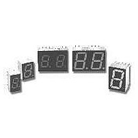
HDSP-G113 Avago Technologies US Inc., HDSP-G113 Datasheet - Page 7
HDSP-G113
Manufacturer Part Number
HDSP-G113
Description
DISPLAY 7SEG 2DIG ALGAAS CC 0.4"
Manufacturer
Avago Technologies US Inc.
Type
Panelr
Specifications of HDSP-G113
Display Type
7-Segment
Common Pin
Common Cathode
Number Of Digits/alpha
2
Size / Dimension
0.90" L x 0.67" W x 0.24" H (22.86mm x 17.02mm x 6.10mm)
Digit/alpha Size
0.40" (10.16mm)
Color
Red
Voltage - Forward (vf) Typ
1.8V
Current - Test
5mA
Millicandela Rating
3.9mcd
Wavelength - Peak
645nm
Power Dissipation (max)
37mW
Package / Case
18-DIP (0.600", 15.24mm)
Number Of Digits
2
Illumination Color
Red
Operating Current
1 mA
Luminous Intensity
650 ucd
Package Type
DIP
Product Length (mm)
22.85mm
Product Height (mm)
6.1mm
Product Depth (mm)
17.02mm
Digit Size (in)
.4in
Character Displayed
Numeric
Viewing Area Height (mm)
10.16mm
Emitting Color
Red
Forward Voltage
2.2V
Test Current (it)
5mA
Forward Current
15mA
Dominant Wave Length
637nm
Power Dissipation
37mW
Total Thickness
6.1mm
Reverse Voltage
15V
Mounting
Through Hole
Operating Temperature Classification
Commercial
Pin Count
18
Configuration
Common Cathode
Number Of Elements
16
Peak Wavelength
645nm
Lead Free Status / RoHS Status
Lead free / RoHS Compliant
Lead Free Status / RoHS Status
Lead free / RoHS Compliant, Lead free / RoHS Compliant


Orange
Device Series
HDSP-
A413
F413
H413
All
Devices
A413
F413
H413
High Efficiency Red
Device Series
HDSP-
A21X
F21X, G21X
H21X, K21X
All
Devices
A21X
F21X, G21X
H21X, K21X
7
Parameter
Luminous Intensity/Segment
(Segment Average)
Forward Voltage/Segment or DP
Peak Wavelength
Dominant Wavelength
Reverse Voltage/Segment or DP
Temperature Coefficient of
V
Thermal Resistance LED
Junction-to-Pin
Parameter
Luminous Intensity/Segment
(Digit Average)
Forward Voltage/Segment or DP
Peak Wavelength
Dominant Wavelength
Reverse Voltage/Segment or DP
Temperature Coefficient of
V
Thermal Resistance LED
Junction-to-Pin
F
F
/Segment or DP
/Segment or DP
[1,2]
[3]
[3]
[1,2]
[4]
[4]
Symbol
I
V
O
O
V
ΔV
RT
Symbol
I
V
O
O
V
ΔV
RT
V
V
F
PEAK
d
R
F
PEAK
d
R
J-PIN
J-PIN
F
F
/°C
/°C
Min.
3.0
Min.
360
420
900
3.0
Typ.
0.70
1.0
2.37
2.0
600
603
30
–2
200
320
345
Typ.
980
5390
1200
2800
3700
2.0
635
626
30
-2
200
320
345
Max.
2.5
Max.
2.5
Units
mcd
V
nm
nm
V
mV/°C
°C/W/
Seg.
Units
μcd
V
nm
nm
V
mV/°C
°C/W/
Seg.
Test Conditions
I
I
I
I
I
Test Conditions
I
I
I
I
I
1/6 Duty Factor
I
I
F
F
F
F
R
F
F
F
F
F
F
R
= 5 mA
= 5 mA
= 10 mA
= 20 mA
= 5 mA
= 20 mA
= 5 mA
= 10 mA
= 60 mA Peak:
= 20 mA
= 100 μA
= 100 μA
Related parts for HDSP-G113
Image
Part Number
Description
Manufacturer
Datasheet
Request
R

Part Number:
Description:
LED DISPLAY HEX 4X7 7.4MM HE RED
Manufacturer:
Avago Technologies US Inc.
Datasheet:

Part Number:
Description:
DISPLAY 4X7 NUM RDP BCD YLW
Manufacturer:
Avago Technologies US Inc.
Datasheet:
Part Number:
Description:
DISPLAY 4X7 HEX HI BRIGHT BCD YW
Manufacturer:
Avago Technologies US Inc.
Datasheet:

Part Number:
Description:
LED 7-SEG 7.6MM CC HE RED RHD
Manufacturer:
Avago Technologies US Inc.
Datasheet:

Part Number:
Description:
LED 7-SEG 7.6MM CA GREEN RHD
Manufacturer:
Avago Technologies US Inc.
Datasheet:

Part Number:
Description:
LED 7-SEG 7.6MM CC GREEN RHD
Manufacturer:
Avago Technologies US Inc.
Datasheet:

Part Number:
Description:
LED 7-SEG 7.6MM CA HE RED RHD
Manufacturer:
Avago Technologies US Inc.
Datasheet:
Part Number:
Description:
LED DISPLAY HEX 4X7 7.4MM GREEN
Manufacturer:
Avago Technologies US Inc.
Datasheet:
Part Number:
Description:
LED DISPLAY HEX 4X7 7.4MM HE RED
Manufacturer:
Avago Technologies US Inc.
Datasheet:

Part Number:
Description:
LED 7-SEG 14.2MM CC HE RED RHD
Manufacturer:
Avago Technologies US Inc.
Datasheet:

Part Number:
Description:
LED BAR GRAPH 10SEG GREEN
Manufacturer:
Avago Technologies US Inc.
Datasheet:

Part Number:
Description:
LED BAR GRAPH 10SEG YELLOW
Manufacturer:
Avago Technologies US Inc.
Datasheet:

Part Number:
Description:
LED 7-SEG 10MM CC GREEN RHD
Manufacturer:
Avago Technologies US Inc.
Datasheet:
Part Number:
Description:
DISPL 4X7 OVERRANGE +/- 1 BCD YW
Manufacturer:
Avago Technologies US Inc.
Datasheet:
Part Number:
Description:
DISPL 4X7 HEX OVERRANGE +/-1 BCD
Manufacturer:
Avago Technologies US Inc.
Datasheet: