HCMS-2921 Avago Technologies US Inc., HCMS-2921 Datasheet - Page 7
HCMS-2921
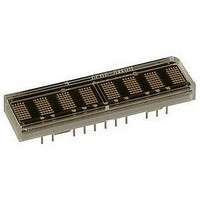
Manufacturer Part Number
HCMS-2921
Description
LED DISPL 5X7 2X8CHAR 3.8MM YLW
Manufacturer
Avago Technologies US Inc.
Series
HCMS-29xxr
Datasheet
1.HCMS-2903.pdf
(16 pages)
Specifications of HCMS-2921
Millicandela Rating
*
Internal Connection
*
Size / Dimension
1.40" L x 0.78" W x 0.20" H (35.6mm x 19.8mm x 5.1mm)
Color
Yellow
Configuration
*
Voltage - Forward (vf) Typ
*
Package / Case
26-DIP
Display Type
Alphanumeric
Number Of Digits/alpha
16
Common Pin
*
Digit/alpha Size
0.15" (3.8mm)
Character Format
Dot Matrix
Character Size
3.81mm
Led Color
Yellow
Luminous Intensity
64µcd
No. Of Digits / Alpha
16
Display Area Width
35.56mm
Display Area Height
19.81mm
Emitting Color
Yellow
Number Of Digits
16
Digit Size (in)
.15in
Viewing Area Height (mm)
3.71mm
Viewing Area Length (mm)
2.11mm
Package Type
DIP
Operating Supply Voltage (min)
3V
Operating Supply Voltage (typ)
5V
Operating Supply Voltage (max)
5.5V
Operating Temperature Classification
Industrial
Operating Temp Range
-40C to 85C
Mounting
Through Hole
Pin Count
28
Total Thickness (mm)
5.08mm
Opto Display Type
Panel
Pattern Type
Dot Matrix
Illumination Color
Yellow
Wavelength
583 nm
Operating Voltage
- 0.3 V to 5.5 V
Maximum Operating Temperature
+ 85 C
Minimum Operating Temperature
- 40 C
Lead Free Status / RoHS Status
Lead free / RoHS Compliant
Lead Free Status / RoHS Status
Lead free / RoHS Compliant, Lead free / RoHS Compliant
Other names
516-1178-5


AC Timing Characteristics Over Temperature Range (-40°C to +85°C)
Timing
Diagram Ref.
Number
1
2
3
4
5
6
7
8
9
10
11
12
Notes:
1. Timing specifications increase 0.3 ns per pf of capacitive loading above 15 pF.
2. This parameter is valid for Simultaneous Mode data entry of the Control Register.
7
Description
Register Select Setup Time to Chip Enable
Register Select Hold Time to Chip Enable
Rising Clock Edge to Falling
Chip Enable Edge
Chip Enable Setup Time to Rising Clock Edge t
Chip Enable Hold Time to Rising Clock Edge
Data Setup Time to Rising Clock Edge
Data Hold Time after Rising Clock Edge
Rising Clock Edge to D
Propagation Delay D
Simultaneous Mode for One IC
CE Falling Edge to D
Clock High Time
Clock Low Time
Reset Low Time
Clock Frequency
Internal Display Oscillator Frequency
Internal Refresh Frequency
External Display Oscillator Frequency
Prescaler = 1
Prescaler = 8
OUT
IN
OUT
to D
Valid
[1]
OUT
[1,2]
t
t
t
t
t
t
t
t
t
t
t
t
F
F
F
F
Symbol
rss
rsh
clkce
ces
ceh
ds
dh
dout
doutp
cedo
clkh
clkl
rstl
cyc
exosc
inosc
rf
4.5 V < V
Min.
10
10
20
35
20
10
10
10
80
80
50
80
150
51.2
410
LOGIC
Max.
40
18
25
5
210
410
1000
8000
<5.5 V
Min.
10
10
20
55
20
10
10
10
100
100
50
80
150
51.2
410
V
LOGIC
= 3 V
Max.
65
30
45
4
210
400
1000
8000
Units
ns
ns
ns
ns
ns
ns
ns
ns
ns
ns
ns
ns
ns
MHz
KHz
Hz
KHz
KHz
Related parts for HCMS-2921
Image
Part Number
Description
Manufacturer
Datasheet
Request
R

Part Number:
Description:
LED DISPLAY 5X7 4CHAR 5MM GREEN
Manufacturer:
Avago Technologies US Inc.
Datasheet:

Part Number:
Description:
LED DISPLAY 5X7 8CHAR 3.8MM YLW
Manufacturer:
Avago Technologies US Inc.
Datasheet:

Part Number:
Description:
LED DISPLAY 5X7 4CHAR 3.8MM YLW
Manufacturer:
Avago Technologies US Inc.
Datasheet:

Part Number:
Description:
LED DISPLAY 5X7 4CHAR 3.8MM ORN
Manufacturer:
Avago Technologies US Inc.
Datasheet:

Part Number:
Description:
LED DISPL 5X7 4CHAR 3.8MM ALGAAS
Manufacturer:
Avago Technologies US Inc.
Datasheet:
Part Number:
Description:
LED DISPLAY 5X7 4CHAR 3.8MM RED
Manufacturer:
Avago Technologies US Inc.
Datasheet:
Part Number:
Description:
LED DISPLAY 5X7 4CHAR 3.8MM ORN
Manufacturer:
Avago Technologies US Inc.
Datasheet:
Part Number:
Description:
LED DISPLAY 5X7 4CHAR 3.8MM YLW
Manufacturer:
Avago Technologies US Inc.
Datasheet:
Part Number:
Description:
LED DISPLAY 5X7 4CHAR 5MM YLW
Manufacturer:
Avago Technologies US Inc.
Datasheet:
Part Number:
Description:
LED DISPLAY 5X7 4CHAR 5MM ORN
Manufacturer:
Avago Technologies US Inc.
Datasheet:
Part Number:
Description:
LED DISPLAY 5X7 4CHAR 5MM GRN
Manufacturer:
Avago Technologies US Inc.
Datasheet:
Part Number:
Description:
LED DISPLAY 5X7 4CHAR 5MM RED
Manufacturer:
Avago Technologies US Inc.
Datasheet:
Part Number:
Description:
LED DISPLAY 5X7 4CHAR 3.8MM RED
Manufacturer:
Avago Technologies US Inc.
Datasheet:
Part Number:
Description:
LED DISPLAY 5X7 4CHAR 3.8MM GRN
Manufacturer:
Avago Technologies US Inc.
Datasheet:
Part Number:
Description:
LED DISPLAY 5X7 4CHAR 5MM GRN
Manufacturer:
Avago Technologies US Inc.
Datasheet: