SLO2016 OSRAM Opto Semiconductors Inc, SLO2016 Datasheet - Page 4
SLO2016
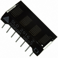
Manufacturer Part Number
SLO2016
Description
INTELLIGENT DISP 4CHAR 5X7 HER
Manufacturer
OSRAM Opto Semiconductors Inc
Datasheet
1.SLG2016.pdf
(10 pages)
Specifications of SLO2016
Display Type
5 x 7 Dot Matrix
Number Of Digits
4
Size / Dimension
0.78" L x 0.40" W x 0.20" H (19.91mm x 10.16mm x 5.08mm)
Color
Red
Character Size
0.18 in
Illumination Color
Super Red
Wavelength
635 nm
Maximum Operating Temperature
+ 85 C
Minimum Operating Temperature
- 40 C
Luminous Intensity
60 ucd
Viewing Area (w X H)
2.54 mm x 4.57 mm
Emitting Color
Sup. Red
Digit Size (in)
.18in
Viewing Area Height (mm)
4.57mm
Viewing Area Length (mm)
2.54mm
Package Type
DIP
Operating Supply Voltage (min)
4.5V
Operating Supply Voltage (typ)
5V
Operating Supply Voltage (max)
5.5V
Operating Temperature Classification
Industrial
Operating Temp Range
-40C to 85C
Mounting
Through Hole
Pin Count
14
Total Thickness (mm)
5.08mm
Opto Display Type
Panel
Pattern Type
Dot Matrix
Lead Free Status / RoHS Status
Lead free / RoHS Compliant
Configuration
-
Voltage - Forward (vf) Typ
-
Millicandela Rating
-
Internal Connection
-
Lead Free Status / Rohs Status
Details
Other names
475-2574
Q68000A8641
SLO2016
Q68000A8641
SLO2016


Pin Function
Pin
1
2
3
4
DC Characteristics at 25°C
Parameters
V
I
I
V
V
I
AC Characteristics (guaranteed minimum timing
parameters at V
Parameter
Address Set
Up Time
Write Time
Data Set Up
Time
Address Hold
Time
Data Hold
Time
Access Time
Clear Disable
Time
Clear Time
Note:
1)
2006-01-23
CC
CC
IL
CC
IL
IH
(all inputs)
T
(all inputs)
(all inputs)
Blank
(80 dots on)
ACC
=Set Up Time + Write Time + Hold Time
Function
WR Write
A1 Digit Select
A0 Digit Select
V
CC
CC
Symbol
T
T
T
T
T
T
T
T
=5.0 V ±0.5 V)
AS
W
DS
AH
DH
ACC
CLRD
CLR
(1)
–40°C
10
60
20
20
20
90
1.0
1.0
Pin
8
9
10
11
+25°C
10
70
30
30
30
110
1.0
1.0
Min.
4.5
—
—
—
2.0
25
Function
D3 Data
D4 Data
D5 Data
D6 Data
SLR2016, SLO2016, SLG2016, SLY2016, SCD5584A
+85°C
10
90
50
40
40
140
1.0
1.0
Typ.
5.0
2.3
80
—
—
—
Unit
ns
ns
ns
ns
ns
ns
µs
ms
4
Max.
5.5
3.0
105
0.8
—
100
Pin Function
Pin
5
6
7
Timing Characteristics—Write Cycle Waveforms
Loading Data
The desired data code (D0–D6) and digit address (A0, A1) must
be held stable during the write cycle for storing new data.
Data entry may be asynchronous. Digit 0 is defined as right hand
digit with A1=A2=0.
Clearing the entire internal four-digit memory can be accomplished
by holding the clear (CLR) low for 1.0 msec minimum. The clear
function will clear the ASCII RAM. Loading an illegal data code will
display a blank.
WR
D0 – D6
A0 – A1
CLR
Function
D0 Data
D1 Data
D2 Data
Units
V
mA
mA
V
V
µA
T
AS
Conditions
—
V
V
4.5 V <V
4.5 V <V
4.5 V <V
CC
CC
=5.0 V
=5.0 V
Pin
12
13
14
CC
CC
CC
T
T
ACC
W
<5.5 V
<5.5 V
<5.5 V, V
T
DS
Function
BL Display Blank
CLR Clear
GND
IN
=0.8 V
T
T
AH
DH
2.0 V
0.8 V
2.0 V
0.8 V
2.0 V
0.8 V
Related parts for SLO2016
Image
Part Number
Description
Manufacturer
Datasheet
Request
R

Part Number:
Description:
INTELLIGENT DISP 4CHAR 5X7 HERED
Manufacturer:
OSRAM Opto Semiconductors Inc
Datasheet:

Part Number:
Description:
DISPLAY 8DIGIT CERAMIC GREEN
Manufacturer:
OSRAM Opto Semiconductors Inc
Datasheet:

Part Number:
Description:
EMITTER IR 950NM 5MM SMD RADIAL
Manufacturer:
OSRAM Opto Semiconductors Inc
Datasheet:

Part Number:
Description:
LED TOPLED GREEN 570NM 2-PLCC
Manufacturer:
OSRAM Opto Semiconductors Inc
Datasheet:

Part Number:
Description:
INTERRUPTER RELFECT W/FILTR SMD
Manufacturer:
OSRAM Opto Semiconductors Inc
Datasheet:

Part Number:
Description:
LED Displays 5x7 Green 0.145 , 4-CHARACTER
Manufacturer:
OSRAM Opto Semiconductors Inc
Datasheet:

Part Number:
Description:
Q65110A4321_SIDELED PURE GREEN EOL150407
Manufacturer:
OSRAM Opto Semiconductors Inc
Datasheet:
Part Number:
Description:
Q65110A1202_RO DETECTOR 3/5MM_TR_RO
Manufacturer:
OSRAM Opto Semiconductors Inc
Datasheet:

Part Number:
Description:
PHOTODIODE 900NM 3MM W/FILTER
Manufacturer:
OSRAM Opto Semiconductors Inc
Datasheet:
Part Number:
Description:
INTELLIGENT DISP 4CHAR 5X7 HERED
Manufacturer:
OSRAM Opto Semiconductors Inc
Datasheet:
Part Number:
Description:
LED TOPLED GREEN 570NM 2-PLCC
Manufacturer:
OSRAM Opto Semiconductors Inc
Datasheet:
Part Number:
Description:
PHOTODIODE 900NM 3MM W/FILTER
Manufacturer:
OSRAM Opto Semiconductors Inc
Datasheet:

Part Number:
Description:
PHOTODIODE 850NM THRU-HOLE
Manufacturer:
OSRAM Opto Semiconductors Inc
Datasheet:

Part Number:
Description:
PHOTODIODE 880NM W/FILTER SMD
Manufacturer:
OSRAM Opto Semiconductors Inc
Datasheet: