HDSP-2133 Avago Technologies US Inc., HDSP-2133 Datasheet - Page 6
HDSP-2133
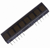
Manufacturer Part Number
HDSP-2133
Description
DISPLAY 5X7 8DIGIT .2" 32DIP GRN
Manufacturer
Avago Technologies US Inc.
Datasheet
1.HDSP-2132.pdf
(16 pages)
Specifications of HDSP-2133
Millicandela Rating
7.5mcd
Color
Green
Configuration
5 x 7
Number Of Digits
8
Character Size
5 mm x 7 mm
Illumination Color
Green
Wavelength
574 nm
Operating Voltage
4.5 V to 5.5 V
Maximum Operating Temperature
+ 85 C
Minimum Operating Temperature
- 55 C
Luminous Intensity
7.5 mcd
Display Type
5 x 7 Dot Matrix
Character Format
Dot Matrix
Led Color
Green
No. Of Digits / Alpha
8
Display Area Width
42.72mm
Display Area Height
9.91mm
Supply Voltage
5V
Rohs Compliant
Yes
Lead Free Status / RoHS Status
Lead free / RoHS Compliant
Size / Dimension
-
Voltage - Forward (vf) Typ
-
Internal Connection
-
Lead Free Status / Rohs Status
Lead free / RoHS Compliant
Other names
516-1745-5
HDSP-2133
HDSP-2133
Available stocks
Company
Part Number
Manufacturer
Quantity
Price
Company:

Part Number:
HDSP-2133
Manufacturer:
TIANBO
Quantity:
3 000


AC Timing Characteristics over Temperature Range
V
Reference
Number
1
2
3
4
5
6
7
8
9
10
11
12
13
–
Notes:
1. Worst case values occur at an IC junction temperature of 150 C.
2. For designers who do not need to read from the display, the Read line can be tied to V
3. Changing the logic levels of the Address lines when CE = “0” may cause erroneous data to be entered into the Character RAM, regardless of the
4. The display must not be accessed until after 3 clock pulses (110 s min. using the internal refresh clock) after the rising edge of the reset line.
6
DD
logic levels of the WR and RD lines.
= 4.5 to 5.5 V unless otherwise specified
Symbol
t
t
t
t
t
t
t
t
t
t
t
t
t
t
ACC
ACS
CE
ACH
CER
CES
CEH
W
WD
DH
R
RD
DF
RC
Description
Display Access Time
Address Setup Time to Chip Enable
Chip Enable Active Time
Address Hold Time to Chip Enable
Chip Enable Recovery Time
Chip Enable Active Prior to Rising Edge of
Chip Enable Hold Time to Rising Edge of
Read/Write Signal
Write Active Time
Data Valid Prior to Rising Edge of Write Signal
Data Write Hold Time
Chip Enable Active Prior to Valid Data
Read Active Prior to Valid Data
Read Data Float Delay
Reset Active Time
Write
Read
Write
Read
Write
Read
[2,3]
[4]
[2,3]
[2,3]
DD
and the Write and Chip Enable lines can be tied together.
[1,2]
Min.
210
230
10
140
160
20
60
140
160
0
100
50
20
160
75
10
300
[1]
Units
ns
ns
ns
ns
ns
ns
ns
ns
ns
ns
ns
ns
ns
ns
Related parts for HDSP-2133
Image
Part Number
Description
Manufacturer
Datasheet
Request
R

Part Number:
Description:
LED 7-SEG 7.6MM CC HE RED RHD
Manufacturer:
Avago Technologies US Inc.
Datasheet:

Part Number:
Description:
LED 7-SEG 7.6MM CA HE RED RHD
Manufacturer:
Avago Technologies US Inc.
Datasheet:

Part Number:
Description:
Seven-Segment Numeric LED Display,2-CHARACTER,Red,DIP
Manufacturer:
Avago Technologies US Inc.
Datasheet:

Part Number:
Description:
Seven-Segment Numeric LED Display,2-CHARACTER,Green,DIP
Manufacturer:
Avago Technologies US Inc.
Datasheet:
Part Number:
Description:
Seven-Segment Numeric LED Display,2-CHARACTER,Green,DIP
Manufacturer:
Avago Technologies US Inc.
Datasheet:
Part Number:
Description:
Seven-Segment Numeric LED Display,2-CHARACTER,Red,DIP
Manufacturer:
Avago Technologies US Inc.
Datasheet:
Part Number:
Description:
Seven-Segment Numeric LED Display,2-CHARACTER,Green,DIP
Manufacturer:
Avago Technologies US Inc.
Datasheet:

Part Number:
Description:
Seven-Segment Numeric LED Display,2-CHARACTER,Orange-Red,DIP
Manufacturer:
Avago Technologies US Inc.
Datasheet:

Part Number:
Description:
LED 7-SEG 14.2MM 2DIG CC HER RHD
Manufacturer:
Avago Technologies US Inc.
Datasheet:

Part Number:
Description:
LED 7-SEG 14.2MM 2DIG CC HER RHD
Manufacturer:
Avago Technologies US Inc.
Datasheet:

Part Number:
Description:
LED 7-SEG 14.2MM 2DIG CA HER RHD
Manufacturer:
Avago Technologies US Inc.
Datasheet:

Part Number:
Description:
LED 7-SEG 14.2MM 2DIG CA GRN RHD
Manufacturer:
Avago Technologies US Inc.
Datasheet:

Part Number:
Description:
LED 7-SEG 14.2MM 2DIG CC GRN RHD
Manufacturer:
Avago Technologies US Inc.
Datasheet:

Part Number:
Description:
LED 7-SEG 14.2MM 2DIG CA GRN RHD
Manufacturer:
Avago Technologies US Inc.
Datasheet:

Part Number:
Description:
LED 7-SEG 14.2MM 2DIG CC GRN RHD
Manufacturer:
Avago Technologies US Inc.
Datasheet: