PD2436 OSRAM Opto Semiconductors Inc, PD2436 Datasheet - Page 10
PD2436
Manufacturer Part Number
PD2436
Description
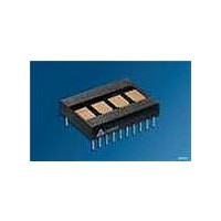
DISPLAY PROGR 4CHAR .20" HE RED
Manufacturer
OSRAM Opto Semiconductors Inc
Series
Alphanumeric Programmable Display™r
Datasheet
1.PD3535.pdf
(14 pages)
Specifications of PD2436
Millicandela Rating
30µcd
Size / Dimension
1.00" L x 0.70" W x 0.20" H (25.40mm x 17.78mm x 5.08mm)
Color
Red
Configuration
5 x 7
Number Of Digits
4
Character Size
0.2 in
Illumination Color
Red
Wavelength
660 nm
Maximum Operating Temperature
+ 85 C
Minimum Operating Temperature
- 40 C
Luminous Intensity
30 ucd
Viewing Area (w X H)
3.56 mm x 5.08 mm
Display Type
5 x 7 Dot Matrix
Lead Free Status / RoHS Status
Lead free / RoHS Compliant
Voltage - Forward (vf) Typ
-
Internal Connection
-
Lead Free Status / Rohs Status
Details
Other names
Q68000A8366


Attributes are non-destructive. If a character with bit D7 set is
replaced by a cursor (Control Word bit D4 is set, and D3=D2=0)
the character will remain in memory and can be revealed again by
clearing D4 in the Control Word.
Blink (D5): The entire display can be caused to blink at a rate of
approximately 2.0 Hz by setting bit D5 in the Control Word. This blink-
ing is independent of the state of D7 in all character locations.
To synchronize the blink rate in a bank of these devices, it is nec-
essary to tie all devices' clocks and resets together as described in
a later section of this data sheet.
Cascading Diagram
2006-01-23
D7
0
0
0
0
0
*“Cursor”= all dots in a single character space lit to half brightness
X = Don't care
B = Depends on the selected brightness.
D6
0
0
0
0
0
D5
0
0
0
0
0
RST
RD
WR
Data I/O
Address
A4
A5
A6
D4
0
1
1
1
1
Decoder
Address
D3
X
0
0
1
1
D0-D7 A0-A2
WR
Programmable Display
D2
X
0
1
0
1
RD
D1
B
B
B
B
B
RST CLK CLK
Address Decode Chip 1 to 14
CE0
D0
B
B
B
B
B
I/O
Operation
Disable high-
light attribute
Display cursor*
instead of
character
Blink single
character
Display blink-
ing cursor*
instead of char-
acter
Alternate char-
acter with cur-
sor*
CE1
SEL
V
CC
14 more displays
in between
10
Lamp Test (D6): When the Lamp Test bit is set, all dots in the
entire display are lit at half brightness. When this bit is cleared, the
display returns to the characters that were showing before the
lamp test.
Clear Data (D7): When D7 is set (D7=1) in the Control Word, all (dis-
play) memory bits are reset to zero and the display goes blank.
A second control word must be written into the chip with D7 reset
(D7=0) to set up attributes and brightness levels.
The SMC- 4740 oscillator is designed to drive up to 16 displays
with input loading of 15 pF each.
The general requirements for cascading 16 displays are:
1.Determine the correct address for each display.
2.Tie CE0 to ground and use CE1 from an address.
3.Select one of the displays to provide the clock for the
4.Tie CLKSEL to ground on other displays.
5.Use RST to synchronize the blinking between the displays.
D7
0
D7
0
D7
1
other displays.
D6
0
D6
1
D6
0
D5
1
D5
0
D5
X
D0-D7
WR
D4
X
D4
X
D4
X
PD243X, PD353X, PD443X
Programmable Display
RD
D3
X
D3
X
D3
X
A0-A2
RST
D2
X
D2
X
D2
X
CE0
D1
B
D1
X
D1
X
CLK
I/O
CE1
D0
B
D0
X
D0
X
CLK
SEL
IDCD5032
Operation
Blinking display
Operation
Lamp test
Operation
Clear
Related parts for PD2436
Image
Part Number
Description
Manufacturer
Datasheet
Request
R

Part Number:
Description:
INTELLIGENT DISP 4CHAR 5X7 HERED
Manufacturer:
OSRAM Opto Semiconductors Inc
Datasheet:

Part Number:
Description:
DISPLAY 8DIGIT CERAMIC GREEN
Manufacturer:
OSRAM Opto Semiconductors Inc
Datasheet:

Part Number:
Description:
EMITTER IR 950NM 5MM SMD RADIAL
Manufacturer:
OSRAM Opto Semiconductors Inc
Datasheet:

Part Number:
Description:
LED TOPLED GREEN 570NM 2-PLCC
Manufacturer:
OSRAM Opto Semiconductors Inc
Datasheet:

Part Number:
Description:
INTERRUPTER RELFECT W/FILTR SMD
Manufacturer:
OSRAM Opto Semiconductors Inc
Datasheet:

Part Number:
Description:
LED Displays 5x7 Green 0.145 , 4-CHARACTER
Manufacturer:
OSRAM Opto Semiconductors Inc
Datasheet:

Part Number:
Description:
Q65110A4321_SIDELED PURE GREEN EOL150407
Manufacturer:
OSRAM Opto Semiconductors Inc
Datasheet:
Part Number:
Description:
Q65110A1202_RO DETECTOR 3/5MM_TR_RO
Manufacturer:
OSRAM Opto Semiconductors Inc
Datasheet:

Part Number:
Description:
PHOTODIODE 900NM 3MM W/FILTER
Manufacturer:
OSRAM Opto Semiconductors Inc
Datasheet:
Part Number:
Description:
INTELLIGENT DISP 4CHAR 5X7 HERED
Manufacturer:
OSRAM Opto Semiconductors Inc
Datasheet:
Part Number:
Description:
LED TOPLED GREEN 570NM 2-PLCC
Manufacturer:
OSRAM Opto Semiconductors Inc
Datasheet:
Part Number:
Description:
PHOTODIODE 900NM 3MM W/FILTER
Manufacturer:
OSRAM Opto Semiconductors Inc
Datasheet:

Part Number:
Description:
PHOTODIODE 850NM THRU-HOLE
Manufacturer:
OSRAM Opto Semiconductors Inc
Datasheet:

Part Number:
Description:
PHOTODIODE 880NM W/FILTER SMD
Manufacturer:
OSRAM Opto Semiconductors Inc
Datasheet: